Method for producing a-IGZO oxide thin film

a thin film, aigzo technology, applied in the direction of chemical vapor deposition coating, synthetic resin layered products, natural mineral layered products, etc., can solve the problems of aperture ratio, increase power consumption, thin film transistor malfunction, etc., and achieve high reproducibility and quality stability. high

Active Publication Date: 2012-04-03
JX NIPPON MINING & METALS CORP
View PDF6 Cites 57 Cited by
  • Summary
  • Abstract
  • Description
  • Claims
  • Application Information

AI Technical Summary

Benefits of technology

[0021]As described above, an embodiment of the invention makes it possible to keep the carrier density of a-IGZO films at a specific value with high reproducibility in a sputtering method suitable for large-area deposition. Thus, thin film transistors and active matrix driving display panels can be provided with high quality stability.

Problems solved by technology

However, silicon-based materials absorb light in the visible light range, so that upon light incidence, they may produce carries to cause thin film transistors to malfunction.
However, such means has disadvantages such as a reduction in aperture ratio or the need to increase the brightness of a backlight for the purpose of keeping the brightness of the screen, which may increase the power consumption.
However, even the production of amorphous silicon films requires a high temperature of about 200° C. or more, which makes it unable to use a polymer film as a substrate, even though the polymer film has advantages such as low cost, light weight, and flexibility.
In addition, the process of manufacturing devices at high temperature has production disadvantages such as high energy cost and time required for heating.
However, the techniques disclosed in the above documents have a problem in that a very small difference in oxygen partial pressure may cause a significant change in the carrier density of films, so that it will be unable to obtain a-IGZO films having the desired carrier density in a stable manner.
In reality, however, it is impossible to control the oxygen concentration with the required accuracy, and therefore, the carrier density of films varies from one production to another, so that films with a constant carrier density cannot be produced with high reproducibility.

Method used


Image

  • Method for producing a-IGZO oxide thin film

Examples


example 1-1

[0076]Indium oxide (In2O3), gallium oxide (Ga2O3) and zinc oxide (ZnO) powders as raw materials were each weighed so that the metal element composition ratio In:Ga:Zn could be 1:1:1. The weighed raw material powders were mixed in a super mixer at a speed of rotation of 3,000 rpm for a time period of 4 minutes in the air. The mixed powder was held in an electric furnace at 1,000° C. for 5 hours in the atmosphere. The calcined powder was placed together with zirconia beads in an attritor and pulverized at a speed of rotation of 300 rpm for a time period of 3 hours. In the pulverization, the average particle size (D50) of the raw material powder reached 0.59 μm. The water content was controlled so that the pulverized raw material powder could form a slurry with a solid content of 50%, and granulation was performed with the inlet temperature set at 200° C. and the outlet temperature set at 120° C. The granulated powder was subjected to press molding under the conditions of a surface pre...

example 2-1

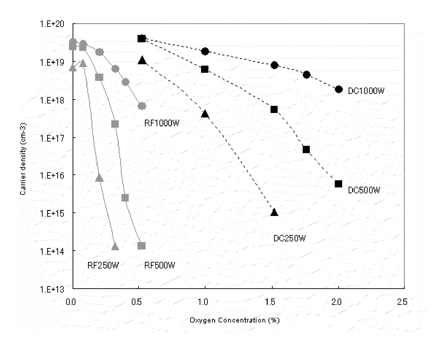
[0081]The sintered material prepared by the method described in Example 1-1 was worked into a disc with a diameter of 6 inches and a thickness of 5 mm, which was used as a sputtering target. The sputtering target and a Corning #1737 glass substrate with a diameter of 4 inches and a thickness of 0.7 mm were placed in a sputtering system, and the sputtering chamber was evacuated to a degree of vacuum of about 5×10⁻⁴ Pa or less by means of a rotary pump and a cryopump. Subsequently, the flow rate of each of pure argon gas and argon gas containing 2% oxygen was controlled by a mass flow controller, so that sputtering gas with an oxygen concentration of 2.0% was introduced into the chamber. The total pressure of the sputtering gas in the chamber was set at 0.5 Pa. A direct current (DC) sputtering method was used with a sputtering power of 1,000 W and a target-substrate distance of 80 mm. The substrate was not heated. The deposition was performed at a rate of 5.29 Å / second for a time peri...

examples 2-2 to 2-10

[0083]The oxide thin films of Examples 2-2 to 2-10 were produced using the sintered material prepared by the method described in Example 1-1 as a sputtering target under the same conditions as in Example 2-1 except for the modifications of the conditions shown in Table 1. All the films had a composition of InGaZnO4 and were amorphous. The results of the measurement of the electrical characteristics of the films are also shown in Table 1.


PUM

PropertyMeasurementUnit
temperatureaaaaaaaaaa

Abstract

There is provided a method for producing an a-IGZO oxide thin film by sputtering, which can control the carrier density of the film to a given value with high reproducibility. The method is an amorphous In—Ga—Zn—O based oxide thin film production method including: providing a sintered oxide material consisting essentially of indium (In), gallium (Ga), zinc (Zn), and oxygen (O) as constituent elements, wherein the ratio [In] / ([In]+[Ga]) of the number of indium atoms to the total number of indium and gallium atoms is from 20% to 80%, the ratio [Zn] / ([In]+[Ga]+[Zn]) of the number of zinc atoms to the total number of indium, gallium and zinc atoms is from 10% to 50%, and the sintered oxide material has a specific resistance of 1.0×10⁻¹ Ωcm or less; and producing a film on a substrate by direct current sputtering at a sputtering power density of 2.5 to 5.5 W / cm2 using the sintered oxide material as a sputtering target.

Description

FIELD OF THE INVENTION[0001]The present invention relates to a method for producing an a-IGZO oxide thin film. More specifically, the invention relates to a method for producing an a-IGZO oxide thin film by a sputtering method using a sputtering target of a sintered oxide material consisting essentially of indium (In), gallium (Ga), zinc (Zn), and oxygen (O) as constituent elements. The invention also relates to methods for manufacturing a transistor and an active matrix driving display panel using the above production method.DESCRIPTION OF THE RELATED ART[0002]Many thin film transistors for applying a driving voltage to drive a display device are used in a display device for various displays such as liquid crystal displays, and their active layers have been produced with silicon-based materials, which have high stability, workability and the like.[0003]However, silicon-based materials absorb light in the visible light range, so that upon light incidence, they may produce carries to...

Claims


Application Information

Patent Timeline
Patent Type & Authority Patents(United States)
IPC IPC(8): H01L21/20H01L21/36
CPCC04B35/453C23C14/086C23C14/3414H01L21/02554H01L21/02565H01L21/02592H01L21/02631H01L29/7869H01L29/66969C04B35/01C04B35/6261C04B35/6263C04B35/62695C04B35/62218C04B2235/77C04B2235/3284C04B2235/3286H01L21/02422C04B2235/5436C04B2235/5445C04B2235/6562C04B2235/6565C04B2235/6567C04B2235/6585Y10T428/31786C23C14/08C23C14/34C04B35/00
Inventor IKISAWA, MASAKATSUYAHAGI, MASATAKA
Owner JX NIPPON MINING & METALS CORP
Why Eureka
Try Eureka