
Photosensitive composition, method for forming pattern, and method for manufacturing semiconductor device

a semiconductor device and composition technology, applied in the field of photosensitive compositions, can solve the problems of reducing the resolution of the photoresist, increasing the roughness of the side wall of the photoresist pattern, and reducing the production yield, so as to reduce the travelling distance of electrons, improve the resolution, and increase the energy per unit area of the photoresist

Active Publication Date: 2012-04-24
RENESAS ELECTRONICS CORP
View PDF34 Cites 2 Cited by
  • Summary
  • Abstract
  • Description
  • Claims
  • Application Information

AI Technical Summary

Benefits of technology

The present invention provides a photosensitive composition that can be irradiated with high energy beam to form a pattern. The composition includes a binder resin and a photoelectron absorbent that can be excited with photoelectron emitted from the binder resin. The absorbent is capable of emitting secondary electron that helps to reduce deterioration in resolution and increases sensitivity of the photoresist. The use of the photosensitive composition allows for the formation of patterned photoresist with enhanced resolution and sensibility, leading to increased productivity in semiconductor manufacturing.

Problems solved by technology

Such line edge roughness is transferred during an etching process for a workpiece to deteriorate a dimensional controllability, and reduces the production yield.
However, the conventional technologies described in the above-described patent publications contains the following problems to be improved.
In other words, additional travelling of about several nanometer is required for attaining a thermal equilibrium for photoelectron, as compared with the conventional lithography, so that the resolution for the photoresist is reduced, causing a problem of increased roughness on the side wall of the photoresist pattern.
Thus, problems in deficient sensibility is caused, in which the amount of light for the exposure is not sufficient for inducing the reaction similarly as in the case of employing the conventional photoresist.

Method used


Image

  • Photosensitive composition, method for forming pattern, and method for manufacturing semiconductor device
  • Photosensitive composition, method for forming pattern, and method for manufacturing semiconductor device
  • Photosensitive composition, method for forming pattern, and method for manufacturing semiconductor device

Examples


example 1

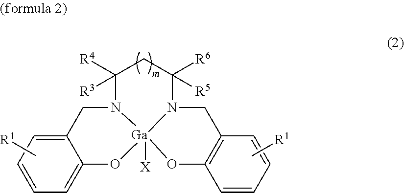
[0108]10 g of substituted polyhydroxystyrene, in which 60% of hydrogen (H) in phenolic hydroxy group is substituted with t-butoxycarbonyl group, 1 g of dimethyl diphenyl gallium, 0.2 g of triphenyl sulfonium trifluoromethanesulfonate, and 0.02 g of diaminodiphenyl methane were dissolved in 120 g of methyl 3-methoxy propionate, and then the solvent was filtered with a filter of 0.2 μm to prepare a composition solution (I). The prepared composition solution was applied over the silicon wafer, and then the wafer was baked at 100 degrees C. for two minutes to form a photoresist film having a thickness of 60 nm. A line-and-space pattern was transferred over the formed photoresist film at 10 mJ / cm2 by employing EUV radiation of a wave length of 13.5 nm, and then a post exposure bake was carried out for two minutes at 90 degrees C., and was developed with tetramethylammonium hydroxide aqueous solution for 60 seconds at 23 degrees C., and then was rinsed with water for 30 seconds. It was fo...

example 2

[0113]The pattern was formed similarly as in Example 1, except that gallium bromide was employed in the preparation of the composition solution (I) employed in Example 1 in place of dimethyl diphenyl gallium and that the different irradiation level of EUV radiation was employed. The sensitivity was 15 mJ / cm2. It was found in an observation of the patterned photoresist by employing a SEM that the above-described line-and-space pattern of a stroke width of 30 nm was successfully resolved. The value of 3 nm was obtained in the measurement of the line edge roughness.

[0114]The results show that respective better values of the sensitivity, the resolution and the line edge roughness were obtained in Example 2, as compared with that obtained in the Comparative Example 1. This manifests that it was found the photoresist pattern was created with higher sensitivity, higher resolution and reduced line edge roughness by employing the lithographic technology presented in Example 2.

example 3

[0115]The pattern was formed similarly as in Example 1, except that gallium chloride-phthalocyanine was employed in the preparation of the composition solution (I) employed in Example 1 in place of dimethyl diphenyl gallium and that the different irradiation level of EUV radiation was employed. The sensitivity was 17 mJ / cm2. It was found in an observation of the patterned photoresist by employing a SEM that the above-described line-and-space pattern of a stroke width of 30 nm was successfully resolved. The value of 2 nm was obtained in the measurement of the line edge roughness.

[0116]The results show that respective better values of the sensitivity, the resolution and the line edge roughness were obtained in Example 3, as compared with that obtained in the Comparative Example 1. This manifests that it was found the photoresist pattern was created with higher sensitivity, higher resolution and reduced line edge roughness by employing the lithographic technology presented in Example 3...


PUM

PropertyMeasurementUnit
wave lengthaaaaaaaaaa
incident energyaaaaaaaaaa
wave lengthaaaaaaaaaa

Abstract

The present invention relates to a photosensitive composition, which is capable of being irradiated with high energy beam having a wave length of 1 to 300 nm band. The photosensitive composition includes a binder resin; and a photoelectron absorbent, capable of being excited with photoelectron emitted from the binder resin that absorbs the high energy beam, when the binder resin is irradiated with the high energy beam.

Description

[0001]This application is based on Japanese patent application No. 2008-160023, the content of which is incorporated hereinto by reference.BACKGROUND[0002]1. Technical Field[0003]The present invention relates to a photosensitive composition, a method for forming pattern, and a method for manufacturing a semiconductor device.[0004]2. Related Art[0005]A lithographic technology is employed as a technology for manufacturing a semiconductor element. A chemically amplified photoresist having a characteristic of higher sensibility is employed in the lithographic technology.[0006]The chemically amplified photoresist contains materials of a binder prepared by introducing a protective group in a base resin, which is soluble to a liquid developer, to reduce the solubility of the resin, and a photosensitive composition composed of a photo-acid generator for generating acid by an irradiation of a high energy ray and the like.[0007]In the lithographic technology employing the chemically amplified...

Claims


Application Information

Patent Timeline
Patent Type & Authority Patents(United States)
IPC IPC(8): G02F7/00G03F7/028G03F7/004
CPCG03F7/0042G03F7/0044G03F7/0382G03F7/0392Y10S430/114Y10S430/127Y10S430/106
Inventor TORIUMI, MINORUITANI, TOSHIRO
Owner RENESAS ELECTRONICS CORP
Learn More