Preparation of copper selenide nanoparticles

a technology of selenide nanoparticles and copper selenide, which is applied in the direction of photovoltaic energy generation, electrical equipment, semiconductor devices, etc., can solve the problems of high cost of single crystal silicon wafers currently used, poor particle size distribution and solubility, and relatively poor light absorption of silicon, etc., to achieve uniform size, confer solubility and/or dispersibility, and narrow melting point range

Active Publication Date: 2015-11-24
NANOCO TECH LTD
View PDF21 Cites 0 Cited by
  • Summary
  • Abstract
  • Description
  • Claims
  • Application Information

AI Technical Summary

Benefits of technology

[0016]Described herein are methods for producing copper selenide nanoparticles by converting a nanoparticle precursor composition containing copper and selenide ions to the material of the copper selenide nanoparticles in the presence of a selenol compound. The method allows control of the copper to selenium stoichiometry and crystallographic phase, yielding essentially monodisperse copper selenide nanoparticles. The resulting nanoparticles have uniform size, and thus, a narrow melting point range. The nanoparticles are capped with an organic ligand to confer solubility and / or dispersibility in organic media, providing processable ink formulations, which can be used to fabricate printable solar cells on flexible substrates. In particular embodiments, the capping ligands can be removed easily at relatively low temperature, thereby enabling low temperature device sintering. Additionally, since in some embodiments the capping ligand can be almost entirely removed under relatively mild heating, the sintered nanoparticles include essentially no carbon residue enabling the fabrication of high performance devices.
[0017]The selenium-rich nanoparticle capping ligand contributes to a selenium-rich atmosphere during sintering, thus avoiding the need for a subsequent selenisation step. Growing the copper selenide nanoparticles this way allows excellent control of the elemental ratio of the sintered copper selenide nanoparticle material. Moreover, the method is scalable to produce large, commercially relevant (e.g. kilogram) quantities of copper selenide nanoparticle material.

Problems solved by technology

Thicker layers are required in silicon-based solar cells because silicon is a relatively poor absorber of light.
Moreover, the single crystal silicon wafers currently used are expensive to produce because the process involves fabricating and then accurately slicing high-purity, single-crystal silicon ingots.
Absorber layers for CIGS photovoltaic devices can be fabricated using a variety of methods, which generally involve expensive vapour phase or evaporation techniques.
However, particle size distribution and solubility are usually very poor.
Existing methods for synthesising copper selenide nanoparticles, as described above, are unfavourable for processing into thin films on a commercial scale as they do not encompass the desirable features of a scalable reaction to generate the required type of nanoparticles having a low melting point, narrow size distribution and a volatile capping ligand.
For instance, hot injection techniques produce materials in very low yields and are not easily scaled commercially.
Other techniques, such as solvothermal or sonochemical syntheses, do not allow tight control over the physical properties of the nanomaterials.
These methods have several drawbacks, including the need to use expensive equipment to generate the high-vacuum required and substrates that can withstand high temperatures.
Further disadvantages are the limited availability of high purity reagents, the reliance upon deposition approaches that are limited to line-of-sight and limited-area sources, which tend to result in poor surface coverage, and, in the case of absorber materials made from more than one element, poor elemental ratio control.

Method used


Image

  • Preparation of copper selenide nanoparticles
  • Preparation of copper selenide nanoparticles
  • Preparation of copper selenide nanoparticles

Examples


example 1

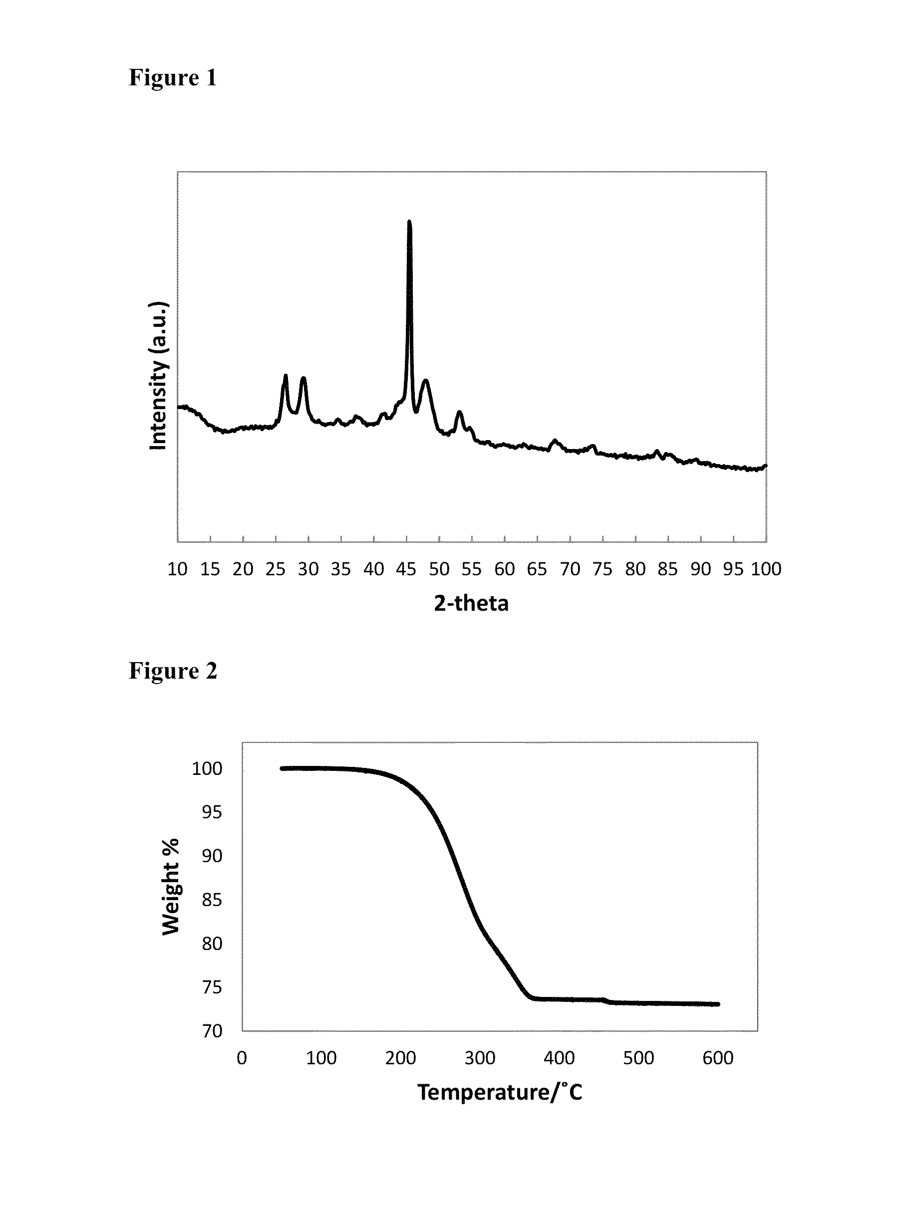
Synthesis of Hexagonal Phase Octane Selenol-Capped Cu2-xSe Nanoparticles

[0073]1.58 g of Cu(ac) (ac=acetate; 0.129 mol) and 12 mL of 1-octadecene were degassed for 30 minutes at 100° C., then 10 minutes at 140° C., before cooling to room temperature under nitrogen flow. The cooled mixture formed a dark green solid. 8 mL of 1-octane selenol (0.0448 mol) was injected into the flask, then the mixture was heated to dissolve the solid and distil off the acetic acid; the flask temperature was raised to 160° C. to completely dissolve the solid. After cooling to 140° C., 8 mL of TOP / Se (1.71 M, 0.0137 mol) was injected into the flask, dropwise, over 8 minutes. Once the addition was complete, the temperature was raised to 160° C. for 2 hours, before annealing at 120° C. for 4 hours, then cooling to room temperature. The solid was isolated by washing with methanol, then acetone, followed by centrifugation. The yellow / brown supernatant was discarded, and the dark brown solid was retained as the...

example 2

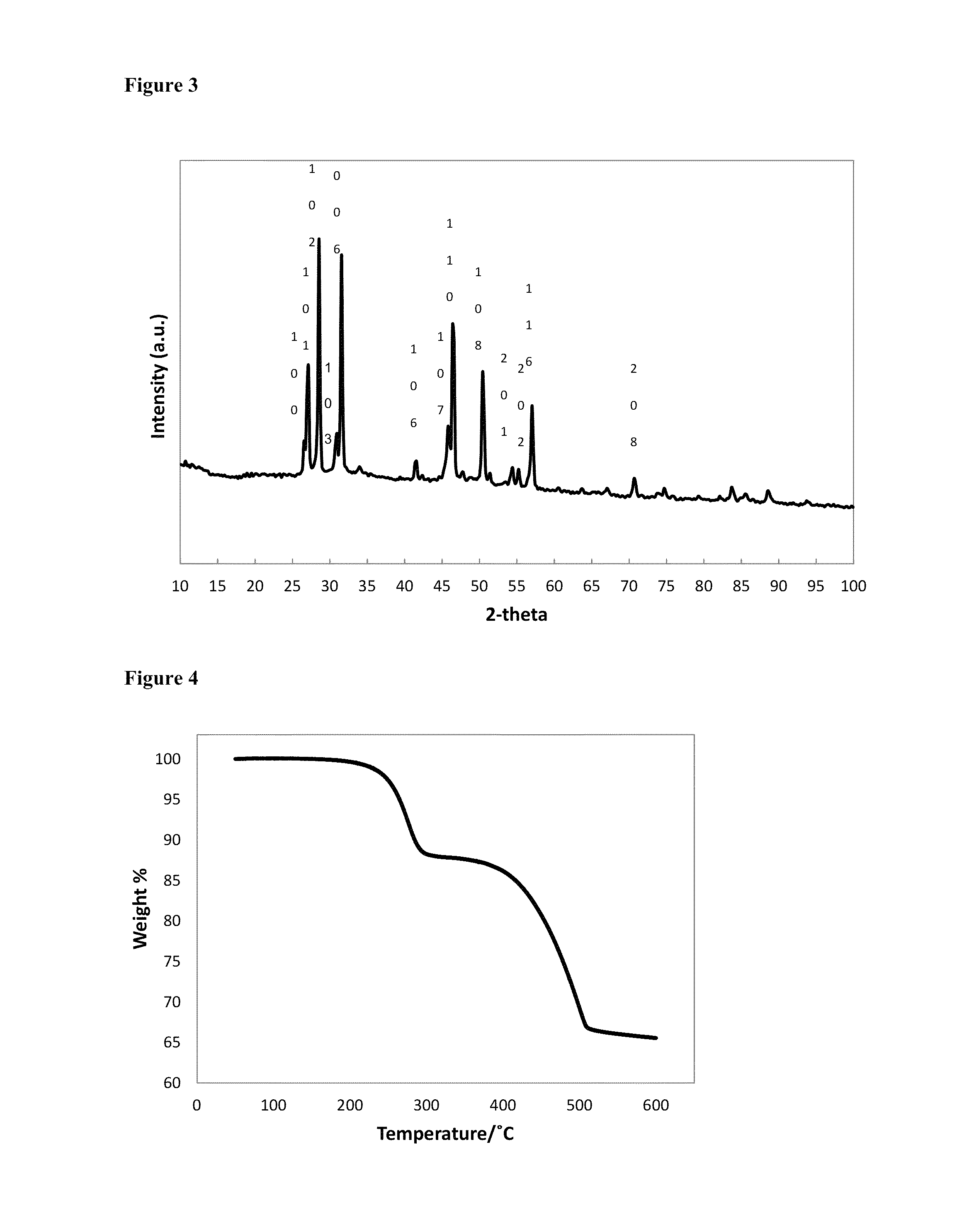
Synthesis of Hexagonal Phase Octane Selenol-Capped CuSe Nanoparticles with the Klockmannite Crystal Structure

[0074]3.88 g of Cu(acac)2 (acac=acetylacetonate; 0.0148 mol), 2.02 g of Se powder (0.0256 mol) and 27 mL of 1-octadecene were degassed for 30 minutes at 100° C., then 10 minutes at 140° C., before cooling to room temperature under nitrogen flow. 16 mL of 1-octane selenol (0.0897 mol), was injected into the flask, then the mixture was heated to 160° C., then held for 2 hours, before annealing at 120° C. for 4 hours, then cooling to room temperature. The solid was isolated by washing with methanol, then acetone, followed by centrifugation. The yellow / green supernatant was discarded, and the fine black powder was retained as the product. Elemental analysis for the product by ICP-OES: C 6.70%; H 1.10%; Cu 40.82%; Se 50.25%. The elemental ratio corresponds to CuSe0.99. FIG. 3 is an XRD pattern for hexagonal phase CuSe capped with 1-octane selenol, as synthesised in Example 2. FIG....

example 3

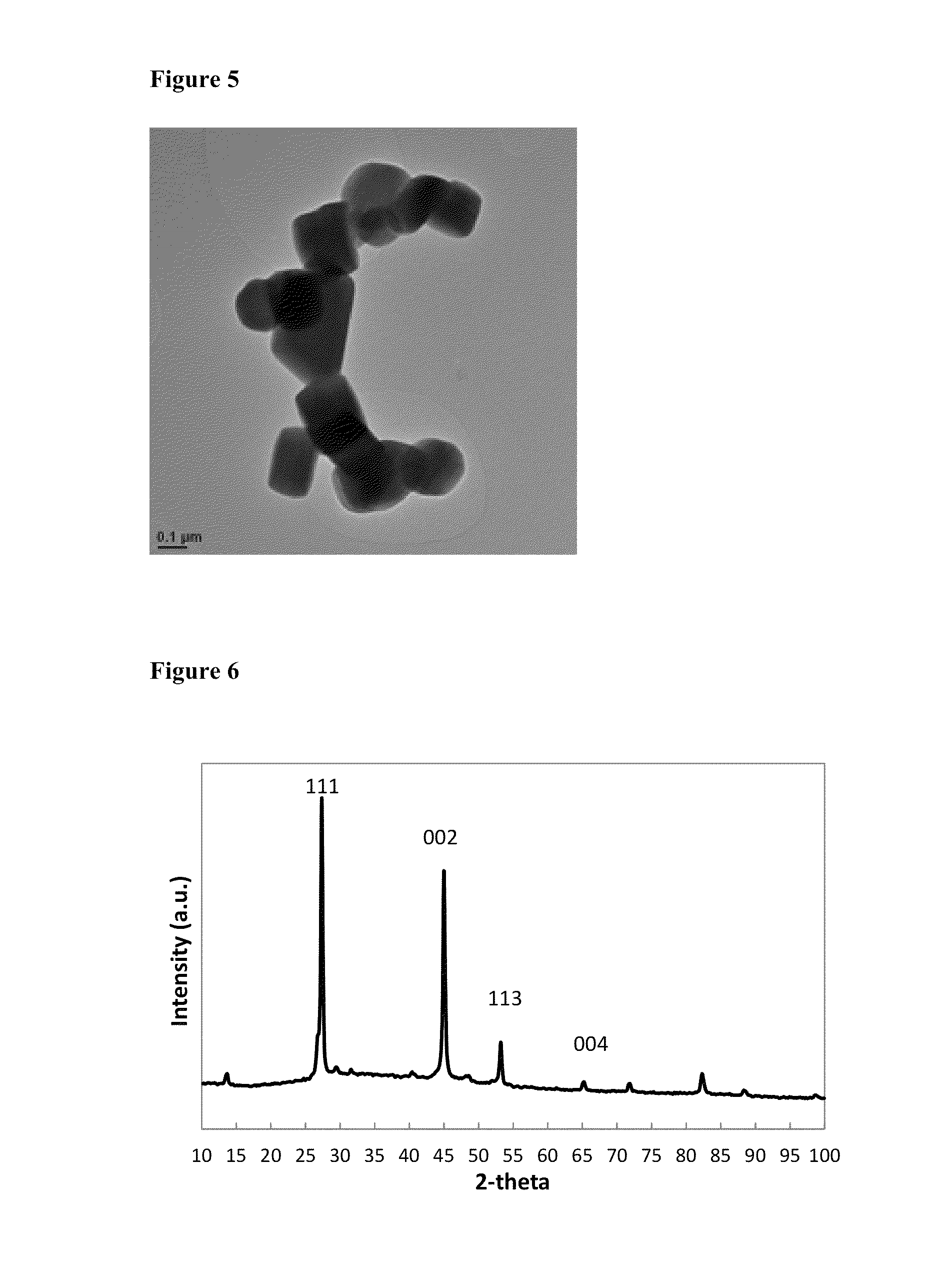
Synthesis of Cubic Phase Octane Selenol-Capped Cu2-xSe Nanoparticles with the Berzelianite Crystal Structure

[0075]3.88 g of Cu(acac)2 (0.0148 mol), 22.5 mL of 1-octadecene and 20.5 mL of 1-octane selenol (0.1149 mol) were degassed for 30 minutes at 100° C., then 10 minutes at 140° C., before cooling to room temperature under nitrogen flow. The mixture was heated to 160° C., then held for 2 hours, before annealing at 120° C. for 4 hours, then cooling to room temperature. The solid was isolated by washing with methanol, then acetone, followed by centrifugation. The yellow / green supernatant was discarded, and the black solid was retained as the product. Elemental analysis for the as-synthesised product by ICP-OES: C 1.56%; H 0.22%; Cu 59.18%; Se 37.78%. The elemental ratio corresponds to Cu1.95Se. Elemental analysis for the product after heating to 600° C.: C 0.03%; H 0.00%; Cu 63.40%; Se 36.49%, suggesting loss of inorganic selenium from the nanoparticles as well as the organo-selenol...


PUM

PropertyMeasurementUnit
absorption coefficientsaaaaaaaaaa
diameteraaaaaaaaaa
diametersaaaaaaaaaa

Abstract

A process for producing copper selenide nanoparticles by effecting conversion of a nanoparticle precursor composition comprising copper and selenide ions to the material of the copper selenide nanoparticles in the presence of a selenol compound. Copper selenide-containing films and CIGS semiconductor films produced using copper selenide as a fluxing agent are also disclosed.

Description

FIELD OF THE INVENTION[0001]The invention relates to materials useful for preparing photovoltaic semiconductor films, and more specifically, to methods of synthesizing copper indium gallium diselenide / sulphide nanoparticles.BACKGROUND[0002]To be commercially viable, photovoltaic cells must generate electricity at a price competitive with fossil fuels. Photovoltaic cells must therefore be fabricated inexpensively using low cost materials and exhibit moderate-to-high efficiency in the conversion of sunlight to electricity. Additionally, the methods used to synthesize the required materials and the device fabrication method must be scalable.[0003]The high cost of crystalline silicon wafers (the industry standard photovoltaic absorber) has led industry to look at cheaper materials to make solar cells. Semiconductors having the formula CuInSe2 or Cu(In,Ga)Se2 (a.k.a. CIGS) materials are strong light absorbers, with absorption coefficients on the order of 105 cm−1. Consequently, the activ...

Claims


Application Information

Patent Timeline
Patent Type & Authority Patents(United States)
IPC IPC(8): H01L21/00H01L31/032H01L31/18H01L21/02H01L51/00
CPCH01L31/032H01L21/02568H01L21/02601H01L21/02628H01L31/0322H01L31/1864H01L51/0091Y02E10/541Y02E10/549H10K85/371H01L31/03923H01L31/0749Y02E10/50
Inventor HARRIS, JAMESGRESTY, NATHALIEMASALA, OMBRETTAPICKETT, NIGEL
Owner NANOCO TECH LTD
Why Eureka
Try Eureka