Pulsed laser induced plasma light source

Active Publication Date: 2016-11-29
KLA TENCOR CORP
View PDF30 Cites 11 Cited by
  • Summary
  • Abstract
  • Description
  • Claims
  • Application Information

AI Technical Summary

Benefits of technology

[0019]In another aspect, a metrology or inspection system suitable for measurement of wafers or reticles includes a repeatedly induced plasma light source as described herein. In some examples, the high brightness illumination light can improve the performance of Spectroscopic Ellipsometry (SE), Spectroscopic Reflectometry (SR), and Beam-Profile Reflectometry (BPR) systems used in film, critical dimension (CD), and composition metrology. Furthermore, the high brightness illumination source described herein can improve the performance of wafer and mask inspection systems employed to detect defects of various types and sizes.
[0020]In one further aspect, a metrology or insp

Problems solved by technology

Without further improvement in NA, the overall defect sensitivity of current metrology tools is limited by the wavelength of the illumination source.
However, these light sources have a number of disadvantages.
For example, electrode based, relatively high intensity discharge arc lamps have radiance limits and power limits due to electrostatic constraints on current density from the electrodes, the limited emissivity of gases as black body emitters, the relatively rapid erosion of electrodes made from refractory materials due to the presence of relatively large current densities at the cathodes, and the inability to control dopants (which can lower the operating temperature of the refractory cathodes) for relatively long periods of time at the required emission current.
However, laser sustained plasma light sources also face significant limitations.
As a result, it is difficult to increase the accessible plasma temperature beyond approximately 12,000-15,000 degrees Kelvin.
Moreover, an increase in laser power generally results in a larger plasma size that has a diminishing impact on color temperature.
Unfortunately, certain metrology system architect

Method used


Image

  • Pulsed laser induced plasma light source
  • Pulsed laser induced plasma light source
  • Pulsed laser induced plasma light source

Examples


Embodiment Construction

[0027]Reference will now be made in detail to background examples and some embodiments of the invention, examples of which are illustrated in the accompanying drawings.

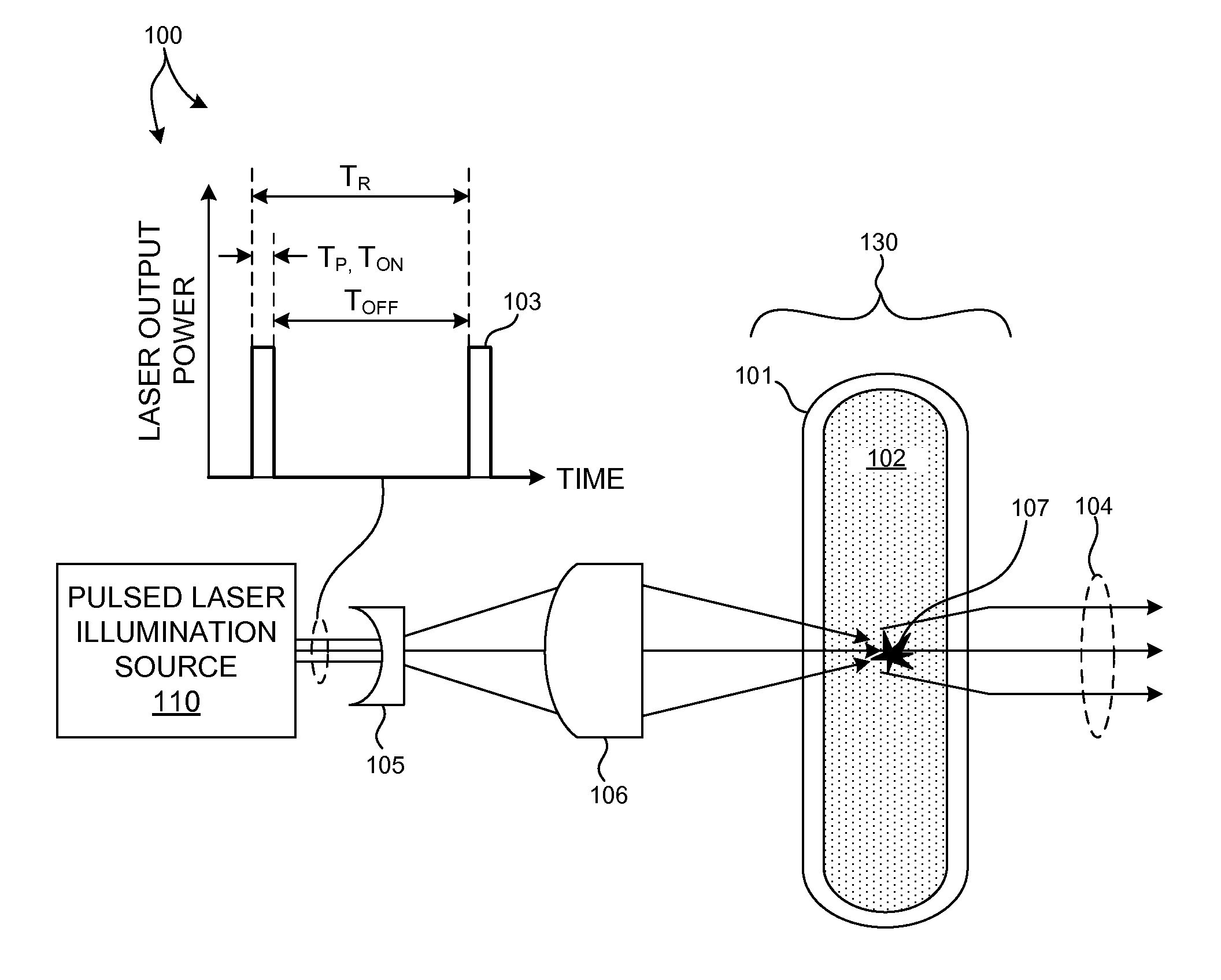
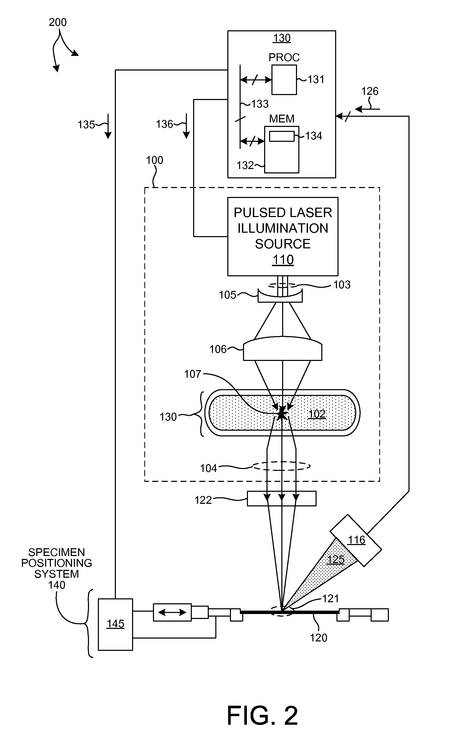
[0028]Methods and systems are described herein for producing high radiance illumination light for use in semiconductor metrology based on repeatedly induced plasma ignition. More specifically, a cold gas is repeatedly ignited by a pulsed laser at a given interval to periodically generate bright plasma. The laser induced plasma light source repeatedly achieves dielectric break-down in a gaseous atmosphere by multi-photon absorption and inverse Bremsstrahlung. A pulse of laser light triggers a break-down event that induces a phase transition from an ordinary state of matter to a plasma state, thus triggering emission of light at high color temperature. After the pulse of laser light, the plasma is extinguished due to a lack of pump energy. This results in a phase transition back to the ordinary state of matter. After th...


PUM


Abstract

Methods and systems are described herein for producing high radiance illumination light suitable for semiconductor metrology. A cold gas is repeatedly ignited by a pulsed laser to periodically generate accessible, high brightness illumination light generated during each break-down event. The pulse duration and repetition period are set to ignite, but not sustain fully formed plasma. The central plasma core emits high color temperature light before a cooler plasma region forms around the central core. Thus, after ignition, the plasma is extinguished before the arrival of the next laser pulse. The repeated plasma ignition/extinction cycle generates illumination light at high color temperature that is accessible for illumination purposes in a metrology application. In one embodiment, a bulb filled with Xenon gas at 10 atmospheres is repeatedly ignited with a pulsed laser having pulse duration of 10 nanoseconds to generate illumination light with a color temperature of approximately 60,000 Kelvin.

Description

CROSS REFERENCE TO RELATED APPLICATION[0001]The present application for patent claims priority under 35 U.S.C. §119 from U.S. provisional patent application Ser. No. 62 / 002,881, entitled “Pulsed Plasma Light Source,” filed May 25, 2014, the subject matter of which is incorporated herein by reference.TECHNICAL FIELD[0002]The described embodiments relate to optical metrology and inspection systems for microscopy, and more particularly to optical metrology and inspection systems involving plasma based radiation sources.BACKGROUND INFORMATION[0003]Semiconductor devices such as logic and memory devices are typically fabricated by a sequence of processing steps applied to a specimen. The various features and multiple structural levels of the semiconductor devices are formed by these processing steps. For example, lithography among others is one semiconductor fabrication process that involves generating a pattern on a semiconductor wafer. Additional examples of semiconductor fabrication pr...

Claims


Application Information

Patent Timeline
IPC IPC(8): G01N21/00G01N21/956G01N21/95G01N21/88F21K99/00G02B27/09H05H1/46
CPCG01N21/8806G01N21/9501G01N21/956F21K99/00H05H1/46G02B27/09G01N2201/0697G01N2021/95676
Inventor FLOCK, KLAUS
Owner KLA TENCOR CORP
Why Eureka
Try Eureka