Electrodeposition apparatus with virtual anode

a virtual anode and electrodeposition technology, applied in the field of selective metal electrodeposition process and apparatus, can solve the problems of metal failure (open circuit) in the hole, increase in line resistance, and affect the ability of metals

Inactive Publication Date: 2002-06-18
PORIS JAIME
View PDF0 Cites 21 Cited by
  • Summary
  • Abstract
  • Description
  • Claims
  • Application Information

AI Technical Summary

Benefits of technology

Briefly, in one preferred embodiment, the present invention is directed toward a process for electrodeposition of metal such as copper, silver or gold into a semiconductor wafer having an active layer such as silicon. The process completes the steps of a diffusion barrier deposition process to provide an electrically conducting layer having contacts and vias on said wafer and to prevent metal diffusion to said silicon, a nucleation layer process to provide a sufficient adhesion surface for the electrodeposited metal, an inert metal mask process to place a first metal mask layer onto said wafer, a selective electrodeposition process to selectively electrodeposit said metal onto said conducting layer of said semiconductor wafer while simultaneously completely filling a contact or via without a standard resist metal etch, a photoresist removal step, and an electrochemical etch process to decrease line-to-line capacitance and simplify planarization processing.

Problems solved by technology

low contact resistance to previous and subsequent metallization steps
These voids can cause an increase in line resistance and ultimately the opening of a line (open circuit).
This directly affects the ability of the metal to carry current into and out of the contacts and vias.
Poor step coverage may lead to the failure (open circuit) of the metal in the hole.
Subsequent processing (planarization and stacking vias on top of contacts) is also complicated by poor step coverage.
They are only partial solutions and introduce other problems such as complicating the metal etch step and increasing the sheet resistance of the metal.
Solving the step coverage problem with standard sputtering techniques has also convincingly failed.
The ability to alloy the aluminum using this technique has not yet been demonstrated nor has its production worthiness.
Hot sputtered aluminum is of questionable production worthiness and electromigration resistance.
Reflowed aluminum requires processing with an expensive laser ($700,000) after standard sputtering.
Blanket LPCVD tungsten is presently economically unattractive as well as exhibiting a much larger resistivity than that of aluminum.
Some economic improvements can be expected, but its large resistance requires thick films which results in large fringing (line to line) capacitances which degrade device performance.
Thick lines and lines with sharp edges and corners also complicate subsequent planarization processing.
Additionally, plasma etching of tungsten has not proven to be as production worthy a process as that of aluminum etching.
Selective LPCVD tungsten plugs with sputtered aluminum addresses the step coverage problem, but has throughput and economic problems, leakage current concerns when used as the first metallization process and electromigration resistance concerns.
Step coverage should be excellent, but electromigration resistance is still an issue.

Method used


Image

  • Electrodeposition apparatus with virtual anode
  • Electrodeposition apparatus with virtual anode
  • Electrodeposition apparatus with virtual anode

Examples


Embodiment Construction

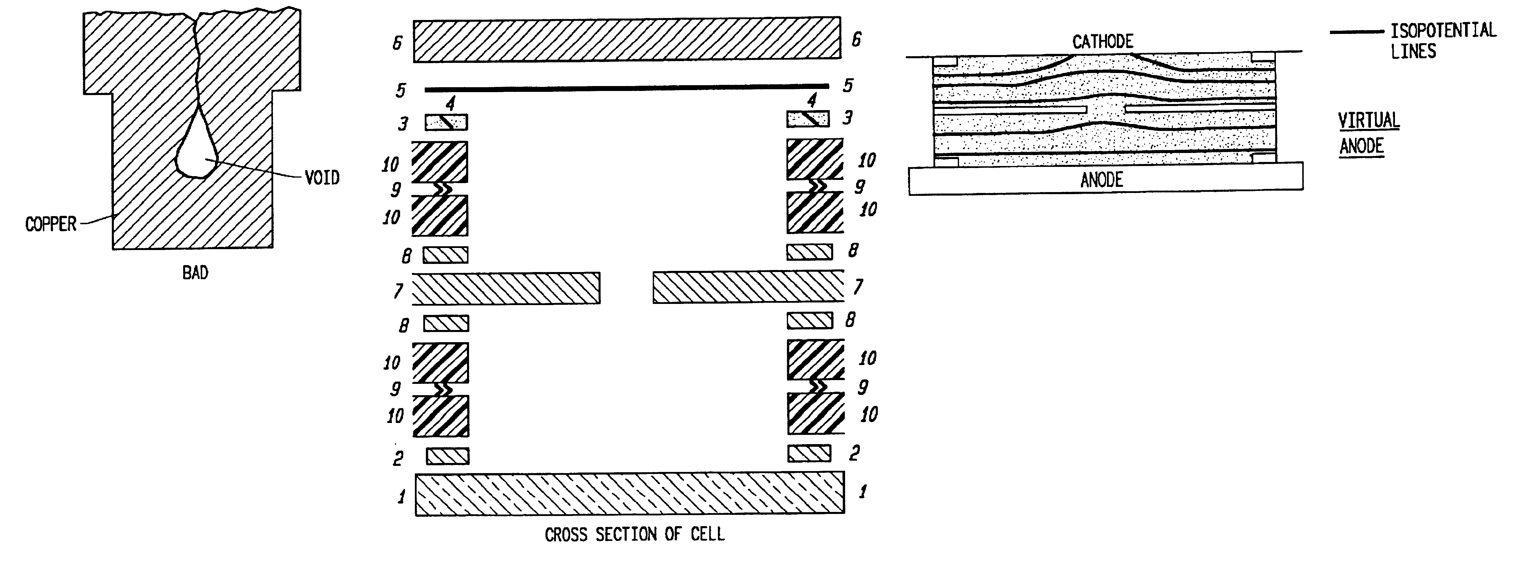
In FIG. 9 the electrode 1 is named the anode (although for a fraction of the time it may be the cathode when pulse plating is employed). A net loss of metal occurs at this electrode, hence the name anode. Phosphorized copper is utilized with copper plating in a sulfuric acid electrolyte (similar to printed circuit board applications). Pure copper may be employed if so desired, but may adversely affect anodic polarization and particulate generation. Other metal systems (such as silver or gold) would use the particular metal as the anode. An inert anode could also be used with the complication of constantly changing the electrolyte composition. The area of this electrode is similar to the area of the exposed wafer.

References in the printed circuit board literature imply that there is an optimum anode current density utilizing the acid copper bath for proper anode passivation. This will depend on the exposed area of the wafer (area without photoresist) as well as the deposition current...


PUM

PropertyMeasurementUnit
thicknessesaaaaaaaaaa
coulombic efficiencyaaaaaaaaaa
current densityaaaaaaaaaa

Abstract

An electrochemical etching step in a semiconductor device fabrication process increases the radius of curvature of edges of metal lines deposited on the semiconductor device. The metal lines are fabricated by forming a mask, electrodepositing the metal, and removing the mask, and the electro-chemical etching step in performed subsequently. The increased radius of curvature of the metal lines simplifies subsequent planarization and decreases line-to-line capacitance, thereby enhancing device performance. In an apparatus for performing the fabrication process, wires sown into a gasket which secures the semiconductor wafer and prevents electrolyte leakage, allows the gasket to function also as a component of the cathode. A more uniform metal deposition is created by a virtual anode, i.e., a metal plate having an aperture and being located between the anode and the cathode.

Description

BACKGROUND OF THE INVENTIONThe present invention relates to a selective metal electrodeposition process and apparatus.Following is a list of the most important requirements for metallization processes for advanced semiconductor processing:low metal resistivity (comparable to or less than that of aluminum)low contact resistance to the active device area (a requirement of the diffusion barrier and not the current carrying metal)low contact resistance to previous and subsequent metallization stepsexcellent contact and via step coverage capabilityacceptable film morphology, adhesion and stress propertiesdecreased line-to-line capacitanceimproved planarization processingcompatibility with planarization processingcompatibility with other processing (such as salicides and dielectric depositions)competitive economics and throughput considerationsexcellent reliability (electromigration and corrosion concerns)environmentally responsible processCOMPARISON WITH CURRENT AND PROPOSED METALLIZATIO...

Claims


Application Information

Patent Timeline
Patent Type & Authority Patents(United States)
IPC IPC(8): H01L21/288H01L21/70H01L21/02H01L21/768
CPCH01L21/2885H01L21/76879H01L21/76885
Inventor PORIS, JAIME
Owner PORIS JAIME
Why Eureka
Try Eureka