Method for realizing gallium nitride ELD vertical structure using metal bounding process

A technology of light-emitting diodes and metal bonding, applied in electrical components, circuits, semiconductor devices, etc., can solve the problems of low product yield and difficulty in obtaining high-quality alloy layers.

Inactive Publication Date: 2007-07-25
SHANGHAI INST OF MICROSYSTEM & INFORMATION TECH CHINESE ACAD OF SCI
View PDF0 Cites 64 Cited by
  • Summary
  • Abstract
  • Description
  • Claims
  • Application Information

AI Technical Summary

Problems solved by technology

But according to our experimental results, metal bonding in the form of eutectic bonding is difficult to obtain a high-quality fully bonded alloy layer in the bonding of a gallium nitride epitaxial layer with a diameter greater than two dimensions and an ideal substrate , so in mass production, the yield rate of the product is not high

Method used


Image

  • Method for realizing gallium nitride ELD vertical structure using metal bounding process
  • Method for realizing gallium nitride ELD vertical structure using metal bounding process

Examples


Embodiment 1

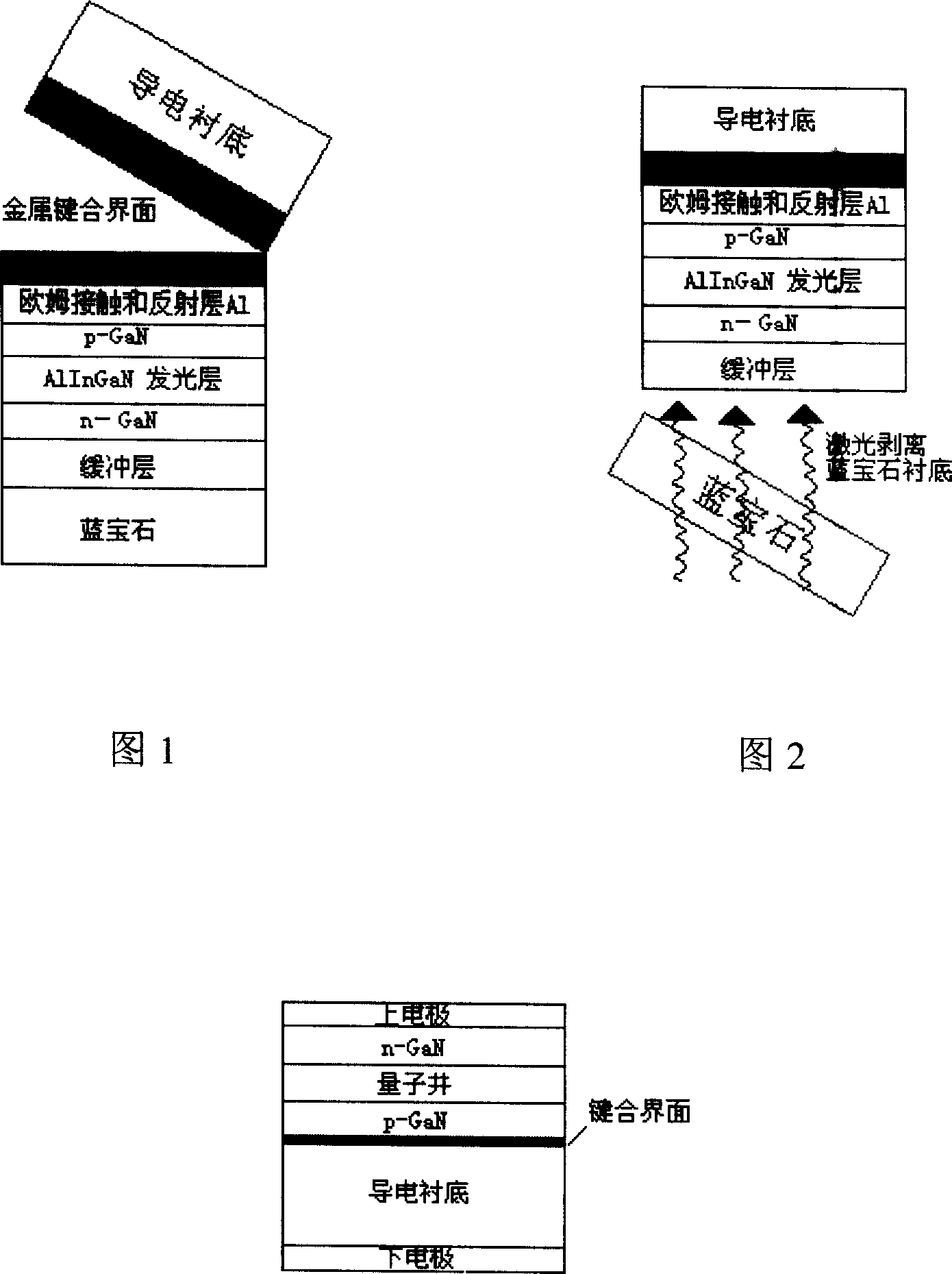
[0022] MOCVD sequentially epitaxy GaN buffer layer, n-type GaN, light-emitting quantum well layer (AlInGaN), p-type GaN on the sapphire substrate

[0023] 2. Thermally evaporate or sputter the metal layer Ni / Au / Al on the p-type gallium nitride layer as the ohmic contact and reflective layer, the thickness of Ni layer and Au layer is 100 Ȧ, and the thickness of Al layer is 1500 Ȧ.

[0024] 3. Thermal evaporation or sputtering of Cr / Au on the reflective layer and on the Si substrate as a bonding interface layer, and the Cr layer as an adhesion layer enables the Au layer to be closely connected to the silicon wafer and prevents the reaction between Au and the substrate Si. Generally, a silicon wafer with good surface flatness is used as the substrate, so that better bonding quality can be obtained when the Au layer is very thin. Generally, the thickness of the Au layer in Au-Au diffusion bonding is about 0.5μ (too thin or too thick metal layer will lead to a decrease in surface f...


PUM

PropertyMeasurementUnit
thicknessaaaaaaaaaa

Abstract

Using metal bonding technique in diffusion bonding form, the method bonds gallium nitride LED developed and prepared on sapphire and silicon chip in low resistance together, and realizes ohmic contact. Advantages are: stable bonding technique, high ratio of good produced parts, small area, using material of luminous layer fully, as well as good conductivity and heat conductivity of substrate.

Description

technical field [0001] The present invention relates to a method for realizing the vertical structure of gallium nitride light-emitting diode (LED) by using metal bonding in the form of diffusion bonding, in particular, realizing the epitaxial gallium nitride LED by using the metal bonding process in the form of diffusion bonding The invention relates to the transfer of devices from sapphire substrates to silicon, copper or other ideal substrates, belonging to the field of optoelectronic materials and devices. Background technique [0002] Gallium nitride is a semiconductor material with a wide bandgap (3.4 electron volts). Many new optoelectronic applications can be developed by utilizing the unique properties of GaN semiconductor materials such as wide bandgap and exciting blue light. At present, GaN optoelectronic devices and electronic devices have good development prospects in the application fields of optical storage, laser printing, high-brightness LEDs and wireless ...

Claims


Application Information

Patent Timeline
Patent Type & Authority Applications(China)
IPC IPC(8): H01L33/00
Inventor 欧欣王曦陈静孙佳胤武爱民
Owner SHANGHAI INST OF MICROSYSTEM & INFORMATION TECH CHINESE ACAD OF SCI
Why Eureka
Try Eureka