Nano doping dielectric material for preparing base-metal inner-electrode multi-layer ceramic sheet type capacitor

A capacitor dielectric and multilayer ceramic technology, which is applied to fixed capacitor dielectrics, multilayer capacitors, components of fixed capacitors, etc., can solve problems such as being unsuitable for mass production, large dielectric temperature coefficient, and unfavorable dielectric layer thinning. , to achieve the effect of simple and adjustable formula, small temperature change rate, and small dielectric loss

Active Publication Date: 2010-06-02
TSINGHUA UNIV
View PDF9 Cites 0 Cited by
  • Summary
  • Abstract
  • Description
  • Claims
  • Application Information

AI Technical Summary

Problems solved by technology

[0004] The composition of this material meets the performance requirements of X7R. The dielectric constant at room temperature can be adjusted from 2000 to 4000, but the sintering temperature is too high, greater than 1300°C, and the dielectric temperature coefficient is relatively large, which is close to -15% at -55°C or -125°C. Not suitable for mass production
In US Patent US-20040229746A1, the basic composition of the ceramic material is BaTiO 3 -Mn 3 o 4 -Y 2 o 3 -Ho 2 o 3 -CaCO 3 -SiO 2 -B 2 o 3 -Al 2 o 3 -MgO-CaO, can be sintered at 1200℃~1300℃, but the ceramic grain is larger than 500nm, which is not conducive to the thinning of the dielectric layer

Method used


Image

  • Nano doping dielectric material for preparing base-metal inner-electrode multi-layer ceramic sheet type capacitor
  • Nano doping dielectric material for preparing base-metal inner-electrode multi-layer ceramic sheet type capacitor
  • Nano doping dielectric material for preparing base-metal inner-electrode multi-layer ceramic sheet type capacitor

Examples


Embodiment 1

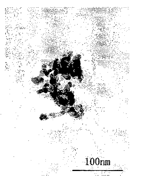
[0062] Embodiment 1 Preparation of nano dopant. According to the molar ratio of Y:Mn:Mg:Si:Ca=5:3:12:7:1, the corresponding weight of soluble salt and ethyl orthosilicate was weighed. According to the sol-gel method nano-dopant preparation process of the present invention, the precursor solution is prepared, firstly dried at 120° C. for 24 hours, and then dried at 140° C. for 6 hours to obtain a xerogel. The obtained xerogel was heat-treated at 800° C. for 3 h, and then ground and sieved to obtain the desired nano-dopant ND1. figure 1 is a transmission electron micrograph of nano-dopants.

Embodiment 2

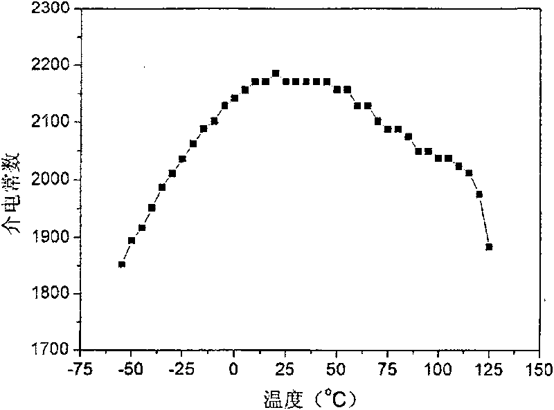
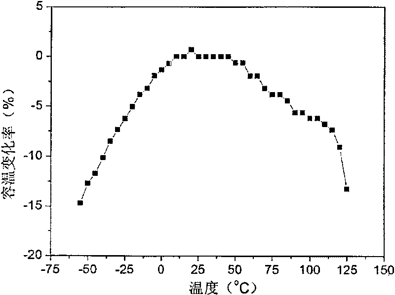
[0063] Embodiment 2 According to BaTiO 3 : 93mol%; (grain size is respectively 110nm, 125nm, 150nm), nano dopant ND1: 7mol% proportioning. The above materials were mixed, ball milled and then dried. After the ceramic material is pressed into a disc, the N 2 / H 2 (20:1) Under reducing atmosphere, sinter at 1200°C for 2h, and then anneal at 1050°C for 2h under weak oxidation conditions. The surface of the sample was covered with a silver electrode, and the electrical performance test was carried out. The dielectric performance parameters are shown in Table 1. figure 2 What the curve provided is the characteristic curve of the dielectric constant of sample 1 of this embodiment 2 changing with temperature, image 3 The curve of the capacitance change rate of sample 1 in Example 2 as a function of temperature is given. Figure 4 It is a scanning electron microscope photo of the surface morphology of sample 1 in Example 2 after sintering. The ceramic grains are spherical and u...

Embodiment 3

[0066] Example 3 Nano-dopants ND2 to ND7 with different components were synthesized according to the sol-gel nano-dopant preparation process provided by the present invention, as shown in Table 2. The doping is performed at 2-10 mol% of the nano dopant relative to the barium titanate, as shown in Table 3. The above materials are mixed, ball milled, and then dried. After the obtained ceramic material is pressed into a disc, the N 2 / H 2 (25:1) Under reducing atmosphere, sinter at 1150-1250°C for 2-3h, then anneal at 1050°C for 3h under weak oxidation conditions. The surface of the sample was covered with a silver electrode, and the electrical performance test was carried out. The dielectric performance parameters are shown in Table 3.

[0067] Table 2

[0068] Dopant No.

Composition (element molar ratio)

ND2

Y: Ce: Mn: Mg: Si: Ca = 4: 1: 3: 12: 5: 2

ND3

Y: Ce: Mn: Mg: Si: Ca = 5: 1: 2.5: 10: 5: 2.5

ND4

Y:Sm:Mn:Mg:Si:Ba=3:1:4.5:10...


PUM

PropertyMeasurementUnit
particle diameteraaaaaaaaaa
thicknessaaaaaaaaaa
particle sizeaaaaaaaaaa

Abstract

The invention discloses a nano coping preparing base metal inner electrode multilayer ceramic plate capacitor dielectric material, which belongs to the capacitor material preparation technical range.The ceramic material consists of main material of BaTiO3 which occupies 90-98 molar portions in a formula and nanodopant which occupies 2-10mol percent of the total weight of the materials. Two-segment sintering or conventional sintering is implemented at the reducing atmosphere and at 950-1250 DEG C to obtain X7R / X5R type MLCC material with perfect performances. The room temperature dielectric constant (round plate sample) of the material can be controlled within 2000-2600, the temperature coefficient of capacitance is less than or equal to about 15 percent, the room temperature dielectric consumption is less than or equal to 1.5 percent, and the size of a grain of the ceramics can be controlled within 100-200nm. The uniformity is good. The invention is applied to the production of multilayer ceramic capacitors with large volume and ultra-thin dielectric layer of less than 3 Mu m thick. And the insulation resistivity is high, and the performance is stable.

Description

technical field [0001] The invention belongs to the technical field of electronic ceramic capacitor materials, and in particular relates to a base metal internal electrode multilayer ceramic chip capacitor dielectric material prepared by nano-doping. In particular, it relates to the manufacture of ultra-fine-grained, temperature-stable base metal internal electrode multilayer ceramic chip capacitor dielectric material with base metal (such as nickel) as the internal electrode. Background technique [0002] With the development trend of miniaturization and large capacity of electronic equipment and products, the application of surface mount technology is becoming more and more extensive. Electronic components for surface mounting are chip components. Multilayer ceramic capacitors are the most widely used type of chip components. Multilayer Ceramic Capacitors (MLCC) for short. It is prepared by a tape-casting-co-firing process, and the dielectric material and the electrode ...

Claims


Application Information

Patent Timeline
Patent Type & Authority Patents(China)
IPC IPC(8): C04B35/462C04B35/624H01G4/12H01G4/30
Inventor 王晓慧田之滨王天李龙土
Owner TSINGHUA UNIV
Why Eureka
Try Eureka