Light packaging member of power machine with high heat transfer efficiency

A technology of high thermal conductivity and power devices, which is applied in semiconductor devices, semiconductor/solid-state device parts, electric solid-state devices, etc., can solve the problems of reducing chip thermal stress, deformation movement, high interface thermal resistance, etc., to reduce thermal stress, Effects of improved heat dissipation performance, reliability and service life

Inactive Publication Date: 2008-12-03
上海芯光科技有限公司 +1
View PDF4 Cites 36 Cited by
  • Summary
  • Abstract
  • Description
  • Claims
  • Application Information

AI Technical Summary

Problems solved by technology

[0005] The purpose of the present invention is to design and overcome the deficiencies of the prior art, to replace the high-density metal substrate with composite materials such as light-weight and high-thermal-conductivity nano-carbon, to reduce the thermal stress generated when

Method used


Image

  • Light packaging member of power machine with high heat transfer efficiency

Examples


Embodiment 1

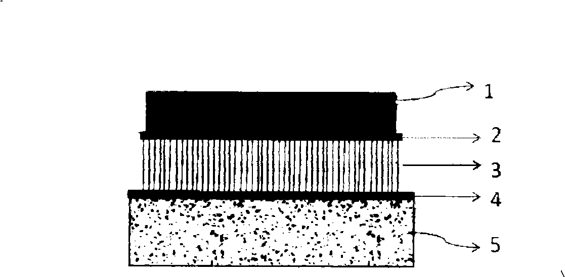
[0013] See attached figure 1 , consisting of an upper high thermal conductivity bonding interface layer 2 , a heat sink film 3 , a lower high thermal conductivity bonding interface layer 4 , and a heat dissipation substrate 5 sequentially bonded on the back of the chip 1 from top to bottom, wherein,

[0014] Bonding interface layers 2 and 4 are metals and their alloy materials with good thermal and electrical conductivity, including Sn, In, Zn, Au, Ag, Cu, Ti, Ni, Al, Mo and their alloys such as CuIn, AgIn, AuIn, InSn , AgSn, AuSn, etc., the above-mentioned bonding interface layer is prepared by magnetron sputtering, evaporation, chemical deposition and other methods; the bonding interface layer 2 and 4 are relatively thin, with a thickness of about 10-100 nanometers, have high thermal conductivity, and are easy to chip 1 is welded with the heat sink film 3 .

[0015] The heat sink film 3 is made of lightweight materials with highly directional thermal conductivity, and mater...

Embodiment 2

[0019] The material of the bonding interface layer 4 in Example 1 is selected from metal thin films including Fe or Co or Ni or Cu or Pd or Ti or Mo materials, with a thickness of 5-50 nanometers. The bonding interface layer 4 can be directly prepared on the surface of the heat dissipation substrate 5 by methods such as sputtering, electroplating, electroless plating, and electron beam evaporation, and then the heat sink film 3 can be directly grown, including conductive and high thermal conductivity carbon nanotube films, carbon nanofiber films, etc. Material. The heat sink film 3 is mainly prepared by methods such as hot wire chemical vapor deposition, plasma chemical vapor deposition or arc plasma deposition, wherein the thermal conductivity of the aligned carbon nanotubes is 600-2000W / m*K, which has a good conductivity.

[0020] The material process of the heat dissipation substrate 5 is the same as that of the first embodiment.

[0021] In this example, the bonding inte...


PUM

PropertyMeasurementUnit
Thicknessaaaaaaaaaa
Thicknessaaaaaaaaaa

Abstract

The invention relates to the technical field of packaging structures of power devices, in particular to a packaging part of a power device with light weight and high efficiency of thermal conductivity, which is characterized in that: an upper high thermal conductivity bonding interface layer, a heat sink thin film, a lower high thermal conductivity bonding interface layer and a radiating substrate are sequentially bonded on the back surface of a chip from top to bottom to form the packaging part; and the radiating substrate adopts high thermal conductivity graphite flake or high thermal conductivity nano-carbon tube/fiber composite material or high thermal conductivity pitch-based carbon-carbon composite material or carbon-copper or carbon-aluminum composite material, or aluminum-based or copper-based silicon carbide or boron nitride or aluminum nitride or silicon nitride ceramic composite material. Compared with the prior art, the back surface of the chip of the invention is directly bonded with the bonding film, the heat sink layer and the radiating substrate, when in work, the heat on the chip is directly guided out of a working region by the three-layer radiating structure, thus enhancing the radiation performance of the product, effectively reducing the heat stress between the chip and the radiating substrate and improving the reliability and the service life of the device.

Description

[technical field] [0001] The invention relates to the technical field of packaging structure of power devices, in particular to a package of light weight and high thermal conductivity power devices. [technical background] [0002] In the field of integrated circuit packaging, there are three development trends of packaging technology: size reduction, function conversion and performance improvement, and technology integration. With the increasing density of integrated circuits, the packaging size is constantly changing. How to effectively dissipate the heat generated by semiconductor chips during operation to ensure the service life and reliability of semiconductor chips has always been a major issue in the semiconductor packaging industry. [0003] In the existing packaging forms, since most of the packaging colloids used to cover semiconductor chips are materials with poor thermal conductivity, such as epoxy resin, etc., due to the low thermal conductivity of the plastic pa...

Claims


Application Information

Patent Timeline
IPC IPC(8): H01L23/36H01L23/367H01L23/373
CPCH01L2924/0002
Inventor 张哲娟孙卓孙鹏
Owner 上海芯光科技有限公司
Why Eureka
Try Eureka