Supercharge Your Innovation With Domain-Expert AI Agents!

Metal master mold for electroforming and use thereof

A metal and master mold technology, applied in electroforming, electrolysis process, etc., can solve problems such as waste, environmental pollution, violent reaction, etc., and achieve the effect of easy removal and cost reduction

Active Publication Date: 2010-12-22
CAPITALBIO CORP +1
View PDF0 Cites 0 Cited by
  • Summary
  • Abstract
  • Description
  • Claims
  • Application Information

AI Technical Summary

Problems solved by technology

At present, the following two methods are usually used to separate the substrate from the electroformed component: one method is to crush the substrate. Although this method is fast, this demolding method is completely destructive, and the commonly used base The chip is a single crystal silicon chip, and the price of a single crystal silicon chip is relatively expensive, and the crushing method causes waste; in addition, the broken substrate is easy to damage the microstructure of the metal component, resulting in the failure of electroforming
Another method is to use an etching method. If the substrate is a silicon wafer, it can be removed with a silicon etchant. It can be removed by etching with a concentrated sodium hydroxide solution at 70°C to 80°C. For a single crystal silicon with a thickness of 300 microns It takes 7-8 hours to corrode; it can also be corroded by hydrofluoric acid and nitric acid at room temperature at a ratio of 1:3, which is very fast, but it is not suitable for common metals such as Ni and Cu, and a large amount of corrosion is produced during the corrosion process. Nitrogen oxide gas, violent reaction, serious pollution
Using corrosion to remove the substrate not only has low processing efficiency, but also uses strong acid or strong alkali to corrode the substrate, which will cause certain environmental pollution.
In addition, if the substrate is glass, the corrosion rate of the glass etchant is very slow, and it is almost the only way to break the substrate

Method used


Image

  • Metal master mold for electroforming and use thereof
  • Metal master mold for electroforming and use thereof
  • Metal master mold for electroforming and use thereof

Examples


Embodiment 1

[0039] Example 1. Preparation of a metal master mold for electroforming of a metal hot-pressing mold for a microfluidic chip

[0040] 1. Making a low melting point metal layer

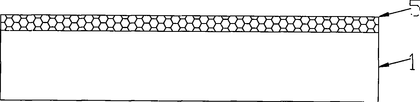
[0041]Deposit 100 on the single crystal silicon wafer 1 Thick titanium, the titanium layer is used as an adhesion layer, and the preparation method is as follows: use a DZS-500 electron beam evaporation coating machine to evaporate 100 For thick titanium, the set parameters are: vacuum degree 9×10 -5 Pa, filament voltage 73V, filament current 0.55A, beam current 53mA; then make a metal indium layer with a thickness of 2 microns, and the indium layer is used as the low melting point metal layer 5 to form figure 1 The structure shown, the metal indium layer preparation method is as follows: using DZS-500 electron beam evaporation coating machine, 100 Metal indium is evaporated on the thick titanium layer, and the set parameters are: vacuum degree 9×10 -5 Pa, filament voltage 80V, filament current ...

Embodiment 2

[0055] Example 2, Preparation of a metal master mold for electroforming of a metal hot-press mold for a microfluidic chip

[0056] 1. Making a low melting point metal layer

[0057] Deposit 100 on the single crystal silicon wafer 1 Thick titanium, the titanium layer is used as an adhesion layer, and the preparation method is as follows: use a DZS-500 electron beam evaporation coating machine to evaporate 100 For thick titanium, the set parameters are: vacuum degree 9×10 -5 Pa, filament voltage 73V, filament current 0.55A, beam current 53mA; then make a metal indium layer with a thickness of 2 microns, and the indium layer is used as the low melting point metal layer 5 to form figure 1 The structure shown, the metal indium layer preparation method is as follows: using DZS-500 electron beam evaporation coating machine, 100 Metal indium is evaporated on the thick titanium layer, and the set parameters are: vacuum degree 9×10 -5 Pa, filament voltage 80V, filament current 0....

Embodiment 3

[0078] Example 3. Preparation of a metal master mold for electroforming of a metal hot-pressing mold for a microfluidic chip

[0079] 1. Making the organic thin film layer

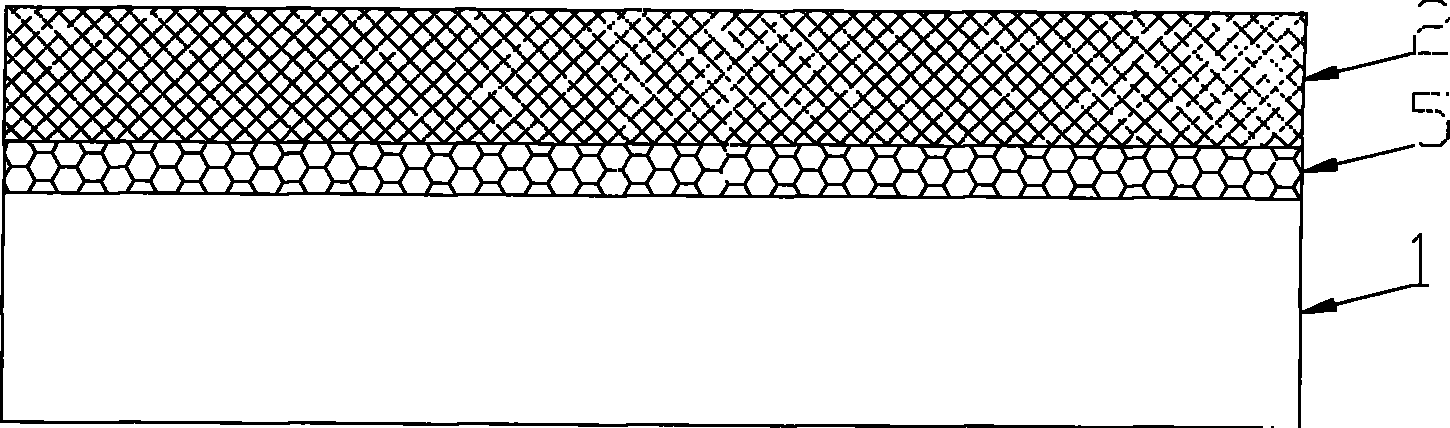
[0080] Put the monocrystalline silicon wafer on the coating machine, and spin-coat BN303 cyclized rubber negative photoresist produced by Beijing Institute of Chemical Reagents, at a speed of 3000rpm, for 30 seconds, and spin-coat to produce a cyclized rubber negative photoresist with a thickness of 1 micron. Resist layer 6, forming Figure 14 structure shown.

[0081] 2. Making a low melting point metal layer

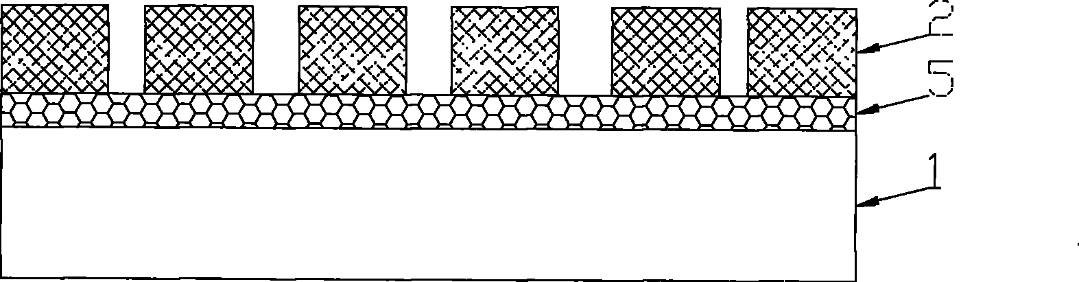
[0082] in having Figure 14 100 Thick titanium, the titanium layer is used as an adhesion layer, and the preparation method of the titanium layer is as follows: use a DZS-500 electron beam evaporation coating machine to evaporate 100 For thick titanium, the set parameters are: vacuum degree 9×10 -5 Pa, filament voltage 73V, filament current 0.55A, beam current 53mA; then make a metal indium...


PUM

PropertyMeasurementUnit
thicknessaaaaaaaaaa

Abstract

The invention discloses a metal master mould used for electrocasting and application thereof. The metal master mould used for electrocasting sequentially comprises a base, an adhesion layer, a low melting point metal layer, a three-dimensional structure layer, the shape of which is matched with that of a target device and a metal seed layer positioned on the whole surface; the low melting point metal layer is any one or a plurality of indium, indium low melting point alloy, tin low melting point alloy, bismuth low melting point alloy, lead low melting point alloy and gallium low melting pointalloy; and the adhesion layer is any one of titanium, chromium and nickel. The metal master mould used for electrocasting can be used for manufacturing metal cast products, the substrate in the metalmaster mould can be removed rapidly, simply and conveniently in the manufacturing process, and the substrate can be kept complete and reused, thus reducing the cost of manufacturing the metal master mould used for electrocasting greatly.

Description

technical field [0001] The invention relates to a metal master mold for electroforming and its application. Background technique [0002] At present, SU8 photoresist is widely used to make master molds with microstructure electroforming components on the surface of silicon wafers. The process of master mold processing and electroforming components is as follows: SU8 photoresist is coated on the surface of the silicon wafer, the SU8 photoresist is photolithographically formed to form a microstructure, and then an electroformed seed metal layer is deposited on the surface of the microstructure to form an electroformed master mold structure . Subsequently, the metal component is electroformed in the above-mentioned master mold, and then the master mold is separated from the electroformed component by an appropriate method to obtain an electroformed component containing a microstructure. [0003] The separation of substrates and electroformed components is currently a difficul...

Claims


Application Information

Patent Timeline
Patent Type & Authority Patents(China)
IPC IPC(8): C25D1/10
Inventor 于中尧李冠男程京
Owner CAPITALBIO CORP
Features
  • R&D
  • Intellectual Property
  • Life Sciences
  • Materials
  • Tech Scout
  • Unparalleled Data Quality
  • Higher Quality Content
  • 60% Fewer Hallucinations
Learn More