Solid electrolytic capacitor

A technology of solid electrolysis and solid electrolyte, applied in the direction of solid electrolytic capacitors, electrolytic capacitors, capacitors, etc., can solve the problems of cracks, thinning, and narrowing of the conductive path in the dielectric layer, and achieve the effect of small leakage current

Active Publication Date: 2009-07-08
SHOWA DENKO KK
View PDF7 Cites 9 Cited by
  • Summary
  • Abstract
  • Description
  • Claims
  • Application Information

AI Technical Summary

Problems solved by technology

The increase in ESR is considered to be due to the softening of the conductive metal layer, which locally thins the conductive metal layer and narrows the conductive path. In addition, the increase in leakage current is considered to be due to the thermal expansion of the exterior material. The resulting mechanical stress is applied to the dielectric layer of the capacitor element, thereby causing damage such as cracks in the dielectric layer

Method used


Image

  • Solid electrolytic capacitor
  • Solid electrolytic capacitor

Examples


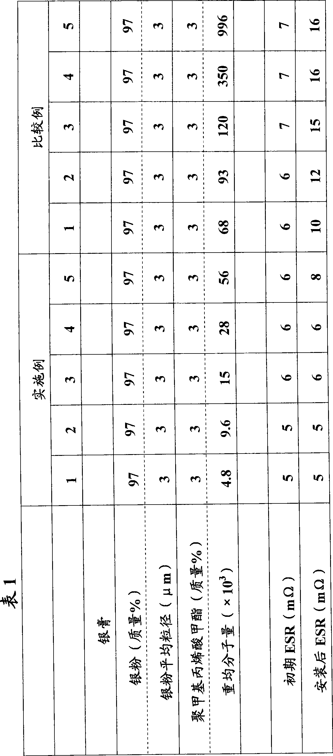
Embodiment 1~5 and comparative example 1~5

[0077] 24.1 mg of tantalum powder and a Φ0.40mm tantalum lead (length 13mm) were molded together, and fired at 1325°C for 20 minutes under vacuum to obtain a CV (product of capacitance and chemical conversion voltage) of 160000μF·V / g , Density is 6.3g / cm 3 , A sintered body with a size of 1.0mm×1.2mm×3.4mm. A tantalum lead of 3.0 mm was buried parallel to the longitudinal direction of the 3.4 mm dimension of the sintered body, and the tantalum lead protruding from the sintered body by 10 mm became an anode part.

[0078] The sintered body was immersed in 1% anthraquinonesulfonic acid aqueous solution at 65°C except for a part of the lead wire, and a voltage of 9V was applied between the sintered body (anode) and the tantalum plate electrode (cathode), and a chemical conversion treatment was performed for 400 minutes. Formed on the surface of the sintered body containing Ta 2 o 5 dielectric layer. A semiconductor (solid electrolyte) layer made of polypyrrole containing naph...

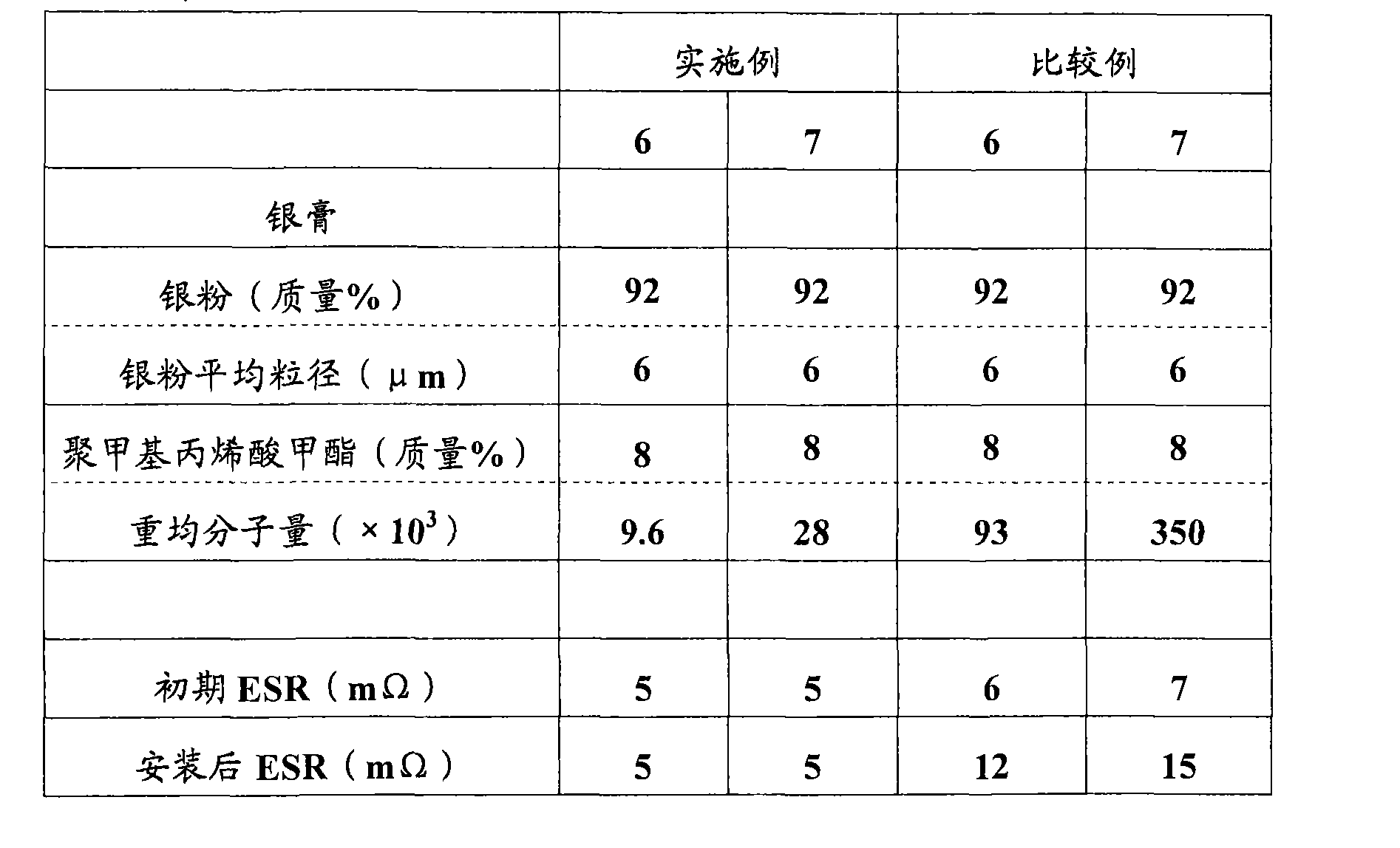
Embodiment 6~7 and comparative example 6~7

[0083] Niobium primary powder (average particle size 0.31 μm) pulverized by utilizing the hydrogen embrittlement of niobium ingot was granulated to obtain niobium powder with an average particle size of 140 μm (because it is a fine powder, the surface is naturally oxidized and contains 9600 ppm oxygen as a whole). Next, by standing in a nitrogen atmosphere at 450°C and then in argon at 700°C, a partially nitrided niobium powder (CV: 285,000 μF·V / g) with a nitrided amount of 9000 ppm was obtained. The partly nitrided niobium powder is molded together with a Φ0.38mm niobium lead (length 13.5mm), and fired at 1260°C to produce multiple pieces with a size of 1.0mm×1.5mm×4.4mm (mass 22.1mg , The niobium lead is buried inside the sintered body with 3.5mm and protrudes 10mm to the outside) of the sintered body.

[0084] Next, the sintered body was immersed in an aqueous solution containing 5% ammonium benzoate and 1% toluenesulfonic acid, and chemical conversion was performed at 20V ...


PUM

PropertyMeasurementUnit
electrical conductivityaaaaaaaaaa
particle sizeaaaaaaaaaa
particle diameteraaaaaaaaaa

Abstract

A dielectric layer and a solid electrolyte layer are formed on the surface of an anode body made of a metal material or a conductive oxide each having a valve action. Subsequently, a conductive carbon paste and a conductive metal paste containing a metal conductive powder and an acrylic resin with a weight-average molecular weight of 60,000 or less are laminated to form a conductive layer, thereby obtaining a solid electrolytic capacitor. The solid electrolytic capacitor is sealed with a resin. In the solid electrolytic capacitor with a large capacitance, even if a thermal stress is received during soldering, the equivalent series resistance (ESR) does not increase and the leakage current does not increase.

Description

technical field [0001] This invention relates to solid electrolytic capacitors. Specifically, it relates to a solid electrolytic capacitor in which the equivalent series resistance (ESR) does not increase and the leakage current does not increase even when subjected to thermal stress during soldering. Background technique [0002] Solid electrolytic capacitors are formed by encapsulating solid electrolytic capacitor elements with resin or the like. The solid electrolytic capacitor element has a structure in which an anode body, a dielectric layer, a solid electrolyte layer, a conductive carbon layer, and a conductive metal layer are sequentially stacked. The anode body is formed, for example, of a porous body obtained by molding and sintering powder of a valve metal. In addition, the dielectric layer is formed of, for example, a dielectric oxide film formed by anodizing the entire surface of the porous body. The anode lead is connected to the anode body in a energizable s...

Claims


Application Information

Patent Timeline
Patent Type & Authority Applications(China)
IPC IPC(8): H01G9/04H01B1/22H01G9/028H01G9/052
CPCH01G11/48Y02E60/13H01G9/15H01G9/0425H01G9/028H01B1/22H01G9/04H01G9/052
Inventor 内藤一美
Owner SHOWA DENKO KK
Why Eureka
Try Eureka