Fast-recovery commutation diode used for high frequency electroplating and production method thereof

A technology of rectifier diodes and manufacturing methods, which is applied in semiconductor/solid-state device manufacturing, circuits, electrical components, etc., can solve the problems of deformation of large-diameter thin silicon wafers, reduce forward and reverse recovery time, and low blocking voltage, and achieve improved Effects of minority carrier life, fast reverse recovery, and high platinum concentration

Active Publication Date: 2009-11-18
JINZHOU SHENGHE POWER ELECTRONICS
View PDF0 Cites 10 Cited by
  • Summary
  • Abstract
  • Description
  • Claims
  • Application Information

AI Technical Summary

Problems solved by technology

[0003] 1) The blocking voltage is low, generally tens of volts, and the voltage of field terminal structures such as field rings and field plates can only reach 200 volts
[0004] 2) Although at low current density (such as JF=10A / cm 2 Below), the forward voltage drop of Schottky power diodes is lower than that of ordinary power diodes, but when JF>10A / cm 2 , the former will be much higher than the latter
Although the voltage is very low (such as 200V, 400V), thin silicon wafers can be used to reduce the forward and reverse recovery time. However, due to the serious deformation of large-diameter thin silicon wafers during diffusion, the current ordinary PiN power diodes must be innovatively modified. In order to achieve the same high frequency application as the Schottky diode

Method used


Image

  • Fast-recovery commutation diode used for high frequency electroplating and production method thereof
  • Fast-recovery commutation diode used for high frequency electroplating and production method thereof
  • Fast-recovery commutation diode used for high frequency electroplating and production method thereof

Examples


Embodiment 1

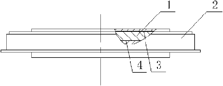
[0031] As shown in the figure, the fast recovery rectifier diode for high-frequency electroplating is composed of a shell 2 and a chip 1, and the chip 1 includes a base area N and a phosphorous expansion area N + and boron expansion area P + And cathode and anode ohmic contacts 3, 4, the chip 1 adopts N-type (100) radial low-resistance monocrystalline silicon wafer, the resistivity ρn of the monocrystalline silicon wafer is 5~9Ω-cm, and the diameter is 48mm , thickness 180±5μm, and pipe thickness 8±0.5mm, phosphorus expansion area N + and boron expansion area P + Formed by double-sided primary diffusion, the cathode and anode ohmic contacts 3 and 4 are titanium-nickel-gold or titanium-nickel-silver.

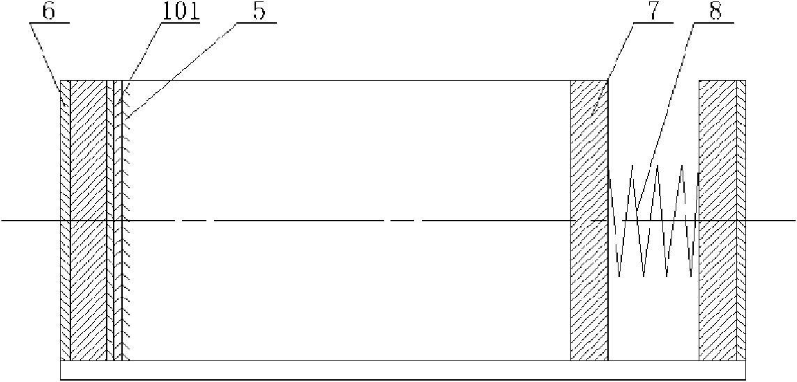
[0032] During manufacture, an N-type (100) radial monocrystalline silicon wafer 101 is used, with a resistivity ρn of 5-9Ω-cm, a diameter of 48mm, and a thickness of 180±5μm; after cleaning, the monocrystalline silicon wafer 101 is placed on On the silicon boat 6, N + ,P + P...

Embodiment 2

[0038] As shown in the figure, the fast recovery rectifier diode for high-frequency electroplating is composed of a shell 2 and a chip 1, and the chip 1 includes a base area N and a phosphorous expansion area N + and boron expansion area P + And cathode and anode ohmic contacts 3, 4, the chip 1 adopts N-type (100) radial low-resistance single crystal silicon wafer, the resistivity pn of the single crystal silicon wafer is 5 ~ 9Ω-cm, and the diameter is 70mm , thickness 180±5μm, and pipe thickness 8±0.5mm, phosphorus expansion area N + and boron expansion area P + Formed by double-sided primary diffusion, the cathode and anode ohmic contacts 3 and 4 are titanium-nickel-gold or titanium-nickel-silver.

[0039] During manufacture, an N-type (100) radial monocrystalline silicon wafer 101 is used, with a resistivity ρn of 5 to 9Ω-cm, a diameter of 70mm, and a thickness of 180±5μm; after cleaning, the monocrystalline silicon wafer 101 is placed on On the silicon boat 6, N + ,P ...

Embodiment 3

[0045] As shown in the figure, the fast recovery rectifier diode for high-frequency electroplating is composed of a shell 2 and a chip 1, and the chip 1 includes a base area N and a phosphorous expansion area N + and boron expansion area P + And cathode and anode ohmic contacts 3, 4, the chip 1 adopts N-type (100) radial low-resistance monocrystalline silicon wafer, the resistivity ρn of the monocrystalline silicon wafer is 5~9Ω-cm, and the diameter is 60mm , thickness 180±5μm, and pipe thickness 8±0.5mm, phosphorus expansion area N + and boron expansion area P + Formed by double-sided primary diffusion, the cathode and anode ohmic contacts 3 and 4 are titanium-nickel-gold or titanium-nickel-silver.

[0046] During manufacture, an N-type (100) radial monocrystalline silicon wafer 101 is used, with a resistivity ρn of 5-9 Ω-cm, a diameter of 60 mm, and a thickness of 180±5 μm; after cleaning, the monocrystalline silicon wafer 101 is placed on On the silicon boat 6, N + ,P ...


PUM

PropertyMeasurementUnit
diameteraaaaaaaaaa
thicknessaaaaaaaaaa
thicknessaaaaaaaaaa

Abstract

The invention relates to a fast-recovery commutation diode used for high frequency electroplating and a production method thereof, wherein the fast-recovery commutation diode has the high frequency property and is suitable for 30KHz/2-5KA/(200-400)V high frequency electroplating with both high voltage and high current density. An N-type (100) radial single crystal silicon piece, which has specific resistance Rho n of 5-9 Ohm-cm, diameter of 48-70 mm and thickness of 175-185 microns, is adopted; silicon piece diffusion is conducted, and double-surface once diffusion is carried out at temperature of 1250 DEG C; the diffusion piece detection is carried out; phosphorosilicate glass and borosilicate glass are used for absorption, the temperature is slowly lowered from 1250 DEG C to 1050 DEG C, the speed rate is 1 DEG C per minute, and isothermal absorption is carried out for 2-3 h; slow temperature reduction is continued till furnace temperature is reduced to 600 DEG C, then furnace delivery is carried out, and minority carrier lifetime Tao p is caused to reach 12-16 Mu S; platinum diffusion is carried out at low temperature so that the minority carrier lifetime Tao p is controlled to be 4-6 Mu S; 12 Mev electron irradiation is carried out so that the minority carrier lifetime Tao p of a base region is 0.9-1.1 Mu S; the two surfaces of the silicon piece are plated with titanium-nickel-gold by means of vapor deposition and then undergo table-board spray sand molding, desanding, cleaning, corrosion, passivation protection, intermediate test, shell arrangement and packaging, and after tests testify qualification, the finished product is produced.

Description

technical field [0001] The invention relates to a fast recovery rectifier diode for high-frequency electroplating with a working frequency of 30KHz, a current of 2-5KA, and a voltage of 200-400V, which can replace the Schottky diode in fast electroplating, and a manufacturing method thereof. Background technique [0002] Schottky power diodes are majority-carrier conductive devices. Since there are no phenomena associated with minority carrier injection, extraction and recombination of excess carriers, they are suitable for making high-frequency power application devices. For low-voltage high-frequency devices, Schottky power diodes have been successfully used for a long time. But Schottky power diodes have the following disadvantages: [0003] 1) The blocking voltage is relatively low, generally tens of volts, and the voltage of field termination structures such as field rings and field plates can only reach 200 volts. [0004] 2) Although at low current density (such as ...

Claims


Application Information

Patent Timeline
Patent Type & Authority Applications(China)
IPC IPC(8): H01L29/861H01L29/04H01L29/06H01L29/16H01L21/22H01L29/45H01L21/329
Inventor 夏吉夫郭永亮潘福泉潘峰
Owner JINZHOU SHENGHE POWER ELECTRONICS
Why Eureka
Try Eureka