Fast-recovery commutation diode used for high frequency electroplating and production method thereof
A technology of rectifier diodes and manufacturing methods, applied in semiconductor/solid-state device manufacturing, circuits, electrical components, etc., can solve the problems of large-diameter thin silicon wafer deformation, low blocking voltage, and reduce forward and reverse recovery time, etc., to achieve improved Effects of minority carrier lifetime, fast reverse recovery, and improved current spreading ability
- Summary
- Abstract
- Description
- Claims
- Application Information
AI Technical Summary
Problems solved by technology
Method used
Image
Examples
Embodiment 1
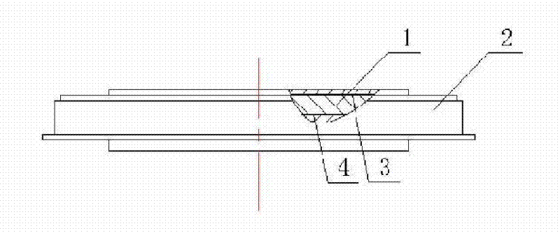
[0031] As shown in the figure, the fast recovery rectifier diode for high-frequency electroplating is composed of a shell 2 and a chip 1, and the chip 1 includes a base area N and a phosphorous expansion area N + and boron expansion area P + And cathode and anode ohmic contacts 3, 4, the chip 1 adopts N-type (100) radial low-resistance monocrystalline silicon wafer, the resistivity ρn of the monocrystalline silicon wafer is 5~9Ω-cm, and the diameter is 48mm , thickness 180±5μm, and pipe thickness 8±0.5mm, phosphorus expansion area N + and boron expansion area P + Formed by double-sided primary diffusion, the cathode and anode ohmic contacts 3 and 4 are titanium-nickel-gold or titanium-nickel-silver.
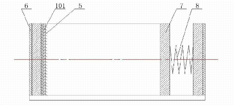
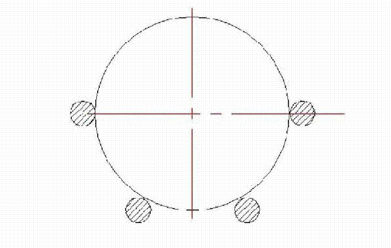
[0032] During manufacture, an N-type (100) radial monocrystalline silicon wafer 101 is used, with a resistivity ρn of 5-9Ω-cm, a diameter of 48mm, and a thickness of 180±5μm; after cleaning, the monocrystalline silicon wafer 101 is placed on On the silicon boat 6, N + ,P + P...
Embodiment 2
[0038] As shown in the figure, the fast recovery rectifier diode for high-frequency electroplating is composed of a shell 2 and a chip 1, and the chip 1 includes a base area N and a phosphorous expansion area N + and boron expansion area P + And cathode and anode ohmic contacts 3, 4, the chip 1 adopts N-type (100) radial low-resistance single crystal silicon wafer, the resistivity pn of the single crystal silicon wafer is 5 ~ 9Ω-cm, and the diameter is 70mm , thickness 180±5μm, and pipe thickness 8±0.5mm, phosphorus expansion area N + and boron expansion area P + Formed by double-sided primary diffusion, the cathode and anode ohmic contacts 3 and 4 are titanium-nickel-gold or titanium-nickel-silver.
[0039] During manufacture, an N-type (100) radial monocrystalline silicon wafer 101 is used, with a resistivity ρn of 5 to 9Ω-cm, a diameter of 70mm, and a thickness of 180±5μm; after cleaning, the monocrystalline silicon wafer 101 is placed on On the silicon boat 6, N + ,P ...
Embodiment 3
[0045] As shown in the figure, the fast recovery rectifier diode for high-frequency electroplating is composed of a shell 2 and a chip 1, and the chip 1 includes a base area N and a phosphorous expansion area N + and boron expansion area P + And cathode and anode ohmic contacts 3, 4, the chip 1 adopts N-type (100) radial low-resistance monocrystalline silicon wafer, the resistivity ρn of the monocrystalline silicon wafer is 5~9Ω-cm, and the diameter is 60mm , thickness 180±5μm, and pipe thickness 8±0.5mm, phosphorus expansion area N + and boron expansion area P + Formed by double-sided primary diffusion, the cathode and anode ohmic contacts 3 and 4 are titanium-nickel-gold or titanium-nickel-silver.
[0046] During manufacture, an N-type (100) radial monocrystalline silicon wafer 101 is used, with a resistivity ρn of 5-9 Ω-cm, a diameter of 60 mm, and a thickness of 180±5 μm; after cleaning, the monocrystalline silicon wafer 101 is placed on On the silicon boat 6, N + ,P ...
PUM
 Abstract
Description
Claims
Application Information


