N-type nano-diamond film and preparation method

A nano-diamond, thin-film technology, applied in metal material coating process, ion implantation plating, coating and other directions, can solve the problems of low carrier mobility, limited application, difficult electronic devices, etc., and achieve high mobility , the method is simple, the effect of low resistivity

Active Publication Date: 2010-06-02
ZHEJIANG UNIV OF TECH
View PDF0 Cites 29 Cited by
  • Summary
  • Abstract
  • Description
  • Claims
  • Application Information

AI Technical Summary

Problems solved by technology

This conduction method makes the film have n-type conduction characteristics with high conductivity and carrier concentration, but low carrier mobility.
The low carrier mobility makes it difficult to form the depletion layer ...

Method used


Image

  • N-type nano-diamond film and preparation method
  • N-type nano-diamond film and preparation method
  • N-type nano-diamond film and preparation method

Examples


Embodiment 1

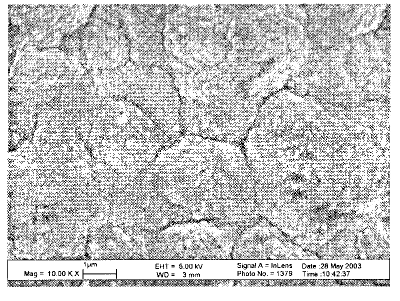
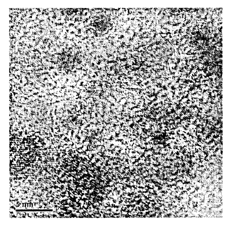
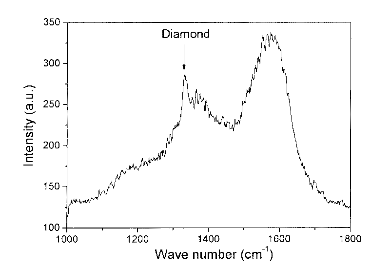
[0030] Polish the monocrystalline silicon wafer with nano-scale diamond powder, and the grinding time is about half an hour. After the polished silicon wafer is cleaned by an ultrasonic machine, it is used as the substrate for the growth of the nano-diamond film. The hot wire chemical vapor deposition method (chemical vapor deposition equipment was purchased from Shanghai Jiaoyou Diamond Coating Co., Ltd.) was used, acetone was used as the carbon source, and acetone was brought into the reaction chamber by hydrogen bubbling. The temperature of the reaction chamber was controlled at 600~ 700° C., the preparation time is 5-6 hours, and a nano-diamond film with a thickness of 3-4 μm is prepared.

[0031] Using a 100keV isotope separator, the implantation energy is 90keV, and the implantation dose in the nano-diamond film is 1015 cm -2 Phosphorus ions and annealed in vacuum at 900 °C for 30 min. The surface of the annealed film was washed with acetone, and then washed with a mix...

Embodiment 2

[0035] The monocrystalline silicon wafer is polished with nanometer diamond powder, and the polishing time is about half an hour. After the polished silicon wafer is cleaned by an ultrasonic machine, it is used as the substrate for the growth of the nano-diamond film. The hot wire chemical vapor deposition method (chemical vapor deposition equipment was purchased from Shanghai Jiaoyou Diamond Coating Co., Ltd.) was used, acetone was used as the carbon source, and acetone was brought into the reaction chamber by hydrogen bubbling. The temperature of the reaction chamber was controlled at 600~ 700° C., the preparation time is 5-6 hours, and a nano-diamond film with a thickness of 3-4 μm is prepared.

[0036] Using a 100keV isotope separator, the implantation energy is 90keV, and the implantation dose in the nano-diamond film is 10 14 cm -2 Oxygen ions (O + , the literature in this field generally uses O + Represents oxygen ions. In the ion implantation process, one electron ...

Embodiment 3

[0040] The monocrystalline silicon wafer is polished with nanometer diamond powder, and the polishing time is about half an hour. After the polished silicon wafer is cleaned by an ultrasonic machine, it is used as the substrate for the growth of the nano-diamond film. The hot wire chemical vapor deposition method (chemical vapor deposition equipment was purchased from Shanghai Jiaoyou Diamond Coating Co., Ltd.) was used, acetone was used as the carbon source, and acetone was brought into the reaction chamber by hydrogen bubbling. The temperature of the reaction chamber was controlled at 600~ 700° C., the preparation time is 5-6 hours, and a nano-diamond film with a thickness of 3-4 μm is prepared.

[0041] Using a 100keV isotope separator, the implantation dose in the nanodiamond film is 10 15 cm -2 Sulfide ion (S + , the literature in this field generally uses S + Indicates sulfur ions. In the ion implantation process, one electron of the atom is generally stripped off to...


PUM

PropertyMeasurementUnit
Diameteraaaaaaaaaa
Resistivityaaaaaaaaaa

Abstract

The invention provides an n-type nano-diamond film and a preparation method. The preparation method comprises the following steps: injecting donor impurity ions into a nano-diamond film by adopting an ion injection method; and performing vacuum annealing on the film to obtain the n-type nano-diamond film. The method uses the ion injection method to finish the step of doping, so that the phosphonium ions or oxonium ions of which the injected dose is 1,014 to 1,016 cm-2 are doped to nano-diamond crystal grains and crystal boundaries, and the defect that impurities are centralized in the crystal boundaries but cannot enter diamond crystal grains in the processes of chemical vapor deposition and doping is avoided; and after the vacuum annealing at the temperature of between 700 and 1,000 DEG C, the n-type diamond film which has lower resistivity and higher Hall mobility is obtained. Therefore, the n-type nano-diamond film has very important scientific significance and engineering value for the application of the film in the field of semiconductor devices, field emission displays, electrochemistry and the like.

Description

(1) Technical field [0001] The invention relates to an n-type nano-diamond thin film and a preparation method thereof. (2) Background technology [0002] Diamond has excellent physical properties such as band gap and high carrier mobility. Compared with electronic materials such as silicon, it can be used in high temperature, high radiation and harsh chemical environments. However, diamond has not been applied in the microelectronics industry at present. The key reason is that it is difficult to prepare n-type diamond films with low resistivity, which makes it difficult to make prototype devices such as pn junctions. The successful preparation of n-type diamond films with high conductivity and the realization of the application of diamond in the microelectronics industry may lead to a revolution in the electronics industry, which has extremely important theoretical and application values. [0003] Over the years, many researchers have searched for impurity elements and dopi...

Claims


Application Information

Patent Timeline
IPC IPC(8): C23C14/06C23C14/48C23C14/58
Inventor 胡晓君
Owner ZHEJIANG UNIV OF TECH
Why Eureka
Try Eureka