Patterning growth method of single-walled carbon nanotubes by surface ruling method

A carbon nanotube and patterning technology, applied in the fields of nanotechnology, nanotechnology, nanostructure manufacturing, etc., can solve the problems of reducing quality, increasing cost, affecting the intrinsic properties of single-wall carbon nanotubes, etc., achieving low cost and operation. simple effect

Inactive Publication Date: 2011-04-20
INST OF METAL RESEARCH - CHINESE ACAD OF SCI
View PDF5 Cites 5 Cited by
  • Summary
  • Abstract
  • Description
  • Claims
  • Application Information

AI Technical Summary

Problems solved by technology

After years of hard work by scientists from various countries, great progress has been made in this direction. For example, the use of transition metal catalysts such as iron, cobalt, and nickel, assisted by electron beam exposure technology, photolithography technology and micro-contact printing technology, has been The positional growth, directional growth and patterned growth of single-walled carbon nanotubes on the surface of silicon substrates can basically be realized, but there are still many difficulties and challenges
For example, the commonly used methods of positional growth and patterned growth of single-walled carbon nanotubes mostly require the help of complex and expensive electron beam exposure technology and photolithography technology, which increases the cost of its industrial production and application.
In addition, almost all current methods for preparing SWNTs use metal catalysts, and the metal impurities remaining in SWNTs are incompatible with existing semiconductor processes and will greatly affect SWNTs The intrinsic physical properties of single-walled carbon nanotubes hinder their application in the field of nanoelectronic devices; the post-treatment purification process can only partially remove the metal catalyst impurities in single-walled carbon nanotubes, and these post-treatment processes will inevitably damage the single-walled carbon nanotubes. The structure of carbon nanotubes causes damage, reducing their quality

Method used


Image

  • Patterning growth method of single-walled carbon nanotubes by surface ruling method
  • Patterning growth method of single-walled carbon nanotubes by surface ruling method
  • Patterning growth method of single-walled carbon nanotubes by surface ruling method

Examples


Embodiment 1

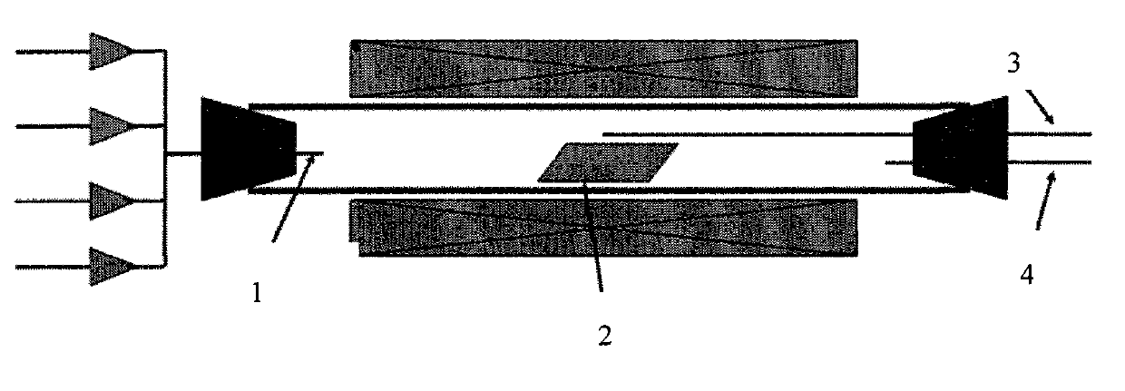
[0025] Such as figure 1 As shown, the device of the present invention adopts a horizontal reaction furnace, the two ends of the horizontal reaction furnace are respectively provided with a gas inlet 1 and a gas outlet 4, and the silicon chip 2 with a thermal oxidation layer is placed in the high temperature zone of the horizontal reaction furnace, and the thermocouple 3 Extend into the high temperature zone of the horizontal reactor to monitor the reaction temperature in real time.

[0026] Silicon wafers with sharp corners are used to score the surface with thermally oxidized SiO 2 layer (10nm) of the silicon substrate to obtain a specific pattern. First, place the silicon substrate in the central area of ​​a horizontal reaction furnace (reaction area, where a thermocouple monitors the furnace temperature in real time); heat it to 850°C in an oxygen atmosphere (the flow rate of oxygen during the heating process is 100 ml / min , heating rate is 40°C / min), oxidation heat treat...

Embodiment 2

[0029] device attached figure 1 .

[0030] Silicon wafers with sharp corners are used to score the surface with thermally oxidized SiO 2 layer (5nm) of the silicon substrate to obtain a specific pattern. First, place the silicon substrate in the central area of ​​a horizontal reactor (reaction zone, where a thermocouple monitors the furnace temperature in real time); heat it to 850°C in an oxygen atmosphere (the oxygen flow rate during the heating process is 200 ml / min , heating rate is 30°C / min), oxidation heat treatment for 10 minutes; then, use 1000 ml / min of argon to exhaust for 8 minutes; (The gas flow rates are respectively 300 ml / min of methane and 500 ml / min of hydrogen), start to grow single-walled carbon nanotubes, and the growth time is 20 minutes.

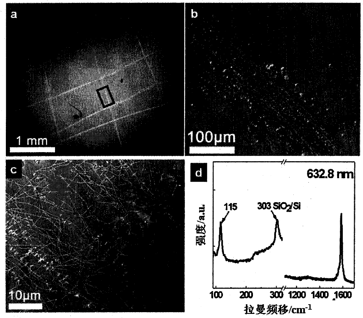
[0031] Scanning electron microscopy, atomic force microscopy and resonance laser Raman spectroscopy observations show that only the scratched area has single-walled carbon nanotubes, which is a randomly distributed n...

Embodiment 3

[0033] device attached figure 1 .

[0034] Silicon wafers with sharp corners are used to score the surface with thermally oxidized SiO 2 layer (10nm) of the silicon substrate to obtain a specific pattern. First, place the silicon substrate in the central area of ​​a horizontal reaction furnace (reaction area, where a thermocouple monitors the furnace temperature in real time); heat it to 850°C in an oxygen atmosphere (the flow rate of oxygen during the heating process is 100 ml / min , heating rate is 40°C / min), oxidative heat treatment for 10 minutes; then, 1000 ml / min of argon gas is used for 8 minutes; into ethanol (wherein, the flow rate of argon is 200 ml / min, and the ethanol is placed in a Montessori washing bottle with a constant temperature of 0 ℃), and hydrogen is introduced as a buffer gas (gas flow rate is 500 ml / min) at the same time, and the growth of single cells is started. Wall carbon nanotubes, the growth time is 20 minutes.

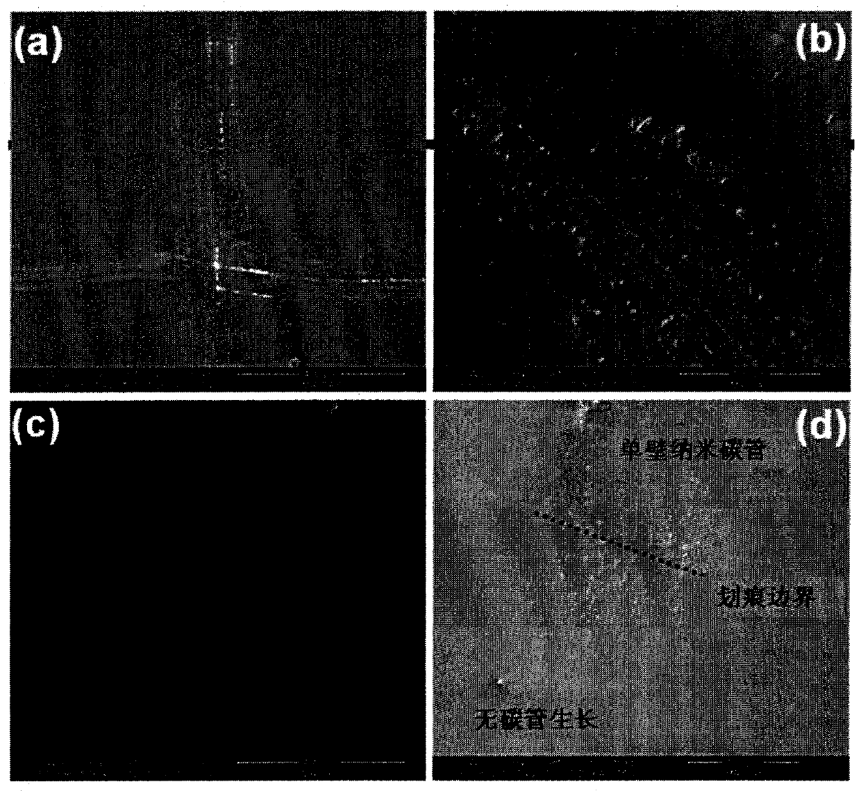
[0035] Scanning electron micros...


PUM

PropertyMeasurementUnit
thicknessaaaaaaaaaa
diameteraaaaaaaaaa
lengthaaaaaaaaaa

Abstract

The invention relates to a patterning preparation technology of single-walled carbon nanotubes, in particular to a patterning growth method of single-walled carbon nanotubes through the surface ruling of a silicon substrate with silicon oxide, which is suitable for the height localizability and the patterning growth of high-quality single-walled carbon nanotubes without impurity residue. The method comprises the following steps of: firstly, ruling the surface of the substrate which is a silicon chip with a thermal oxide layer with a sharp object into a certain pattern to generate a plurality of catalytic active sites in substrate surface localization; then, forming nucleating points of the single-walled carbon nanotubes through high-wetting oxidation treatment; and preparing the single-walled carbon nanotubes through the schizolysis of a carbon source at 600-1,100 DEG C. The invention realizes the location and the patterning growth of the high-quality single-walled carbon nanotubes without any metal impurities in a simple silicon substrate ruling mode, has the advantages of simple and convenient operation, low cost, good localizability and easy patterning and lays a foundation for the application of the single-walled carbon nanotubes in the fields of nano electronic devices, sensors, and the like.

Description

Technical field: [0001] The invention relates to a patterned preparation technology of carbon nanotubes, specifically a method for positioning and patterning growth of single-walled carbon nanotubes on the surface of a silicon substrate by using simple surface scribing, which is suitable for positioning and patterning preparation of carbon nanotubes that do not contain High quality SWNTs contaminated by any metallic impurities. Background technique: [0002] Single-walled carbon nanotubes have excellent electrical, optical, thermal and mechanical properties, making them have broad application prospects in the fields of nanoelectronic devices, optoelectronic devices, sensors, catalyst supports, composite materials, drug delivery and biomedicine. Therefore, since the discovery of carbon nanotubes, their theoretical research and application exploration have always been frontier and hot issues in the fields of physical chemistry and materials science at home and abroad. Single-...

Claims


Application Information

Patent Timeline
Patent Type & Authority Applications(China)
IPC IPC(8): B82B3/00C01B31/02
Inventor 成会明任文才刘碧录
Owner INST OF METAL RESEARCH - CHINESE ACAD OF SCI
Why Eureka
Try Eureka