

Method for preparing anti-reflection layer and anti-reflection surface, photoelectric conversion device used by same
A technology of photoelectric conversion device and anti-reflection layer, which is used in photovoltaic power generation, circuits, electrical components, etc.
- Summary
- Abstract
- Description
- Claims
- Application Information
AI Technical Summary
Problems solved by technology
Method used
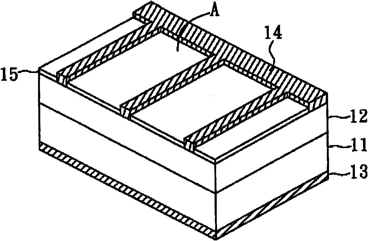
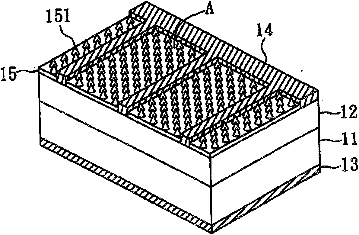
Image

Examples
Embodiment 1
[0030] See Figure 2A to Figure 2E , which is an anti-reflection layer fabrication process for fabricating a sub-wavelength anti-reflection structure on a silicon wafer.
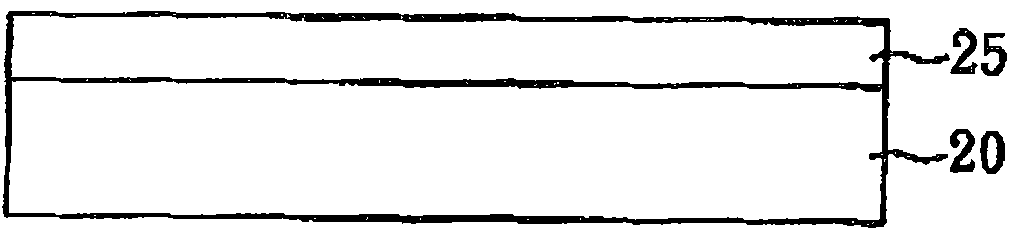
[0031] Such as Figure 2A As shown, the (100) silicon wafer 20 is first cleaned with dilute hydrofluoric acid to remove the native oxide layer on the surface; then, 200± 5 nm thick passivation layer 25 . In this embodiment, the passivation layer 25 is a silicon nitride layer.
[0032] Subsequently, if Figure 2B As shown, a metal film 26 with a thickness of 15±0.5 nm is plated on the surface of the passivation layer 25 by an E-beam evaporating system. In this embodiment, the material of the metal film 26 is nickel.
[0033] Such as Figure 2C As shown, hydrogen and nitrogen gas with a flow rate of 3 sccm are introduced, and the metal film 26 is self-assembled into metal nanoparticles 26' due to surface tension by rapid temperature rise annealing (heating at 850° C. for 60 seconds) as an etching passiva...
Embodiment 2
[0037] The production process of this embodiment is roughly the same as that described in Example 1, except that the material of the metal film in this embodiment is gold, and the heat treatment condition of the metal film is also to heat at 850°C for 60 seconds, and finally use An etchant composed of potassium iodide and iodine removes metal nanoparticles.
experiment example
[0041] The experimental sample that embodiment 1 is made with comparative example 1 to 3 is carried out the comparison of reflectivity, and its result please refer to Figure 4 . Such as Figure 4 As shown, the blank silicon wafer (comparative example 1) without processing all has quite high reflectivity (> 35%) for the wavelength of visible light and near-infrared ray; The long wavelength has lower reflectivity (35%) at 400nm; The long wavelength region has a low reflectance of 20%) in the short wavelength region of 400nm; and the silicon nitride sub-wavelength structure (embodiment 1) shows <10% reflectance, and the wavelength reflectance of 580nm-680nm is reduced to below 1%.
[0042] It can be seen from the above that the anti-reflection layer provided by the present invention has excellent anti-reflection effect, so it can be used in a photoelectric conversion device to increase the amount of light taken to obtain a high-efficiency photoelectric conversion device. Acc...
PUM
| Property | Measurement | Unit |
|---|---|---|
| Thickness | aaaaa | aaaaa |
| Diameter | aaaaa | aaaaa |
| Height | aaaaa | aaaaa |
Abstract
Description
Claims
Application Information