Preparation of Copper Indium Gallium Selenium Thin Films by Photoelectrochemical Deposition

A photoelectrochemical, copper indium gallium selenide technology, applied in the field of solar cell preparation, can solve the problems of poor morphology, difficult indium and gallium deposition, slow film growth rate, etc., achieves low cost, easy large-area deposition, and overcomes the growth rate slow effect

Inactive Publication Date: 2011-12-07
CENT SOUTH UNIV
View PDF4 Cites 21 Cited by
  • Summary
  • Abstract
  • Description
  • Claims
  • Application Information

AI Technical Summary

Problems solved by technology

[0005] The purpose of the present invention is to overcome the problems of slow film growth, difficult deposition of indium and gallium, and poor morphology when preparing copper indium gallium selenide thin films by traditional electrodeposition, and now prov...

Method used


Image

  • Preparation of Copper Indium Gallium Selenium Thin Films by Photoelectrochemical Deposition
  • Preparation of Copper Indium Gallium Selenium Thin Films by Photoelectrochemical Deposition
  • Preparation of Copper Indium Gallium Selenium Thin Films by Photoelectrochemical Deposition

Examples


Embodiment 1

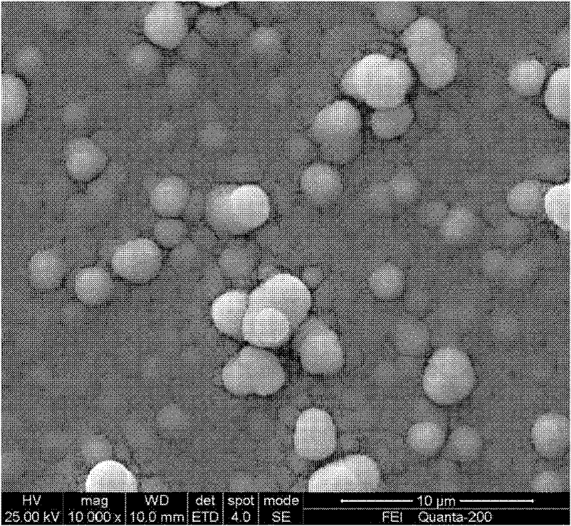
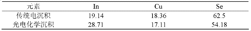
[0025] First, when the solute composition is 0.30mol / L H 2 SeO 3 , in the 500ml aqueous solution of 1mol / L Potassium chloride, adjust pH to 0.3 with dilute hydrochloric acid or sodium hydroxide; Adopt photoelectric cell, with stainless steel substrate as working electrode, large-area Pt net is counter electrode, saturated calomel electrode ( SCE) is the reference electrode; the following photoelectrochemical deposition parameters are adopted: the incident light is a monochromatic light source of 250 nm (the light intensity is 0.1 mW cm -2 ), the working electrode potential was 0.5V (vsSCE), the electrolyte temperature was 80°C, and the deposition time was 10 minutes. A thin film containing selenium with a thickness of 1-1.5 microns is pre-deposited on the cathode substrate. Then, when the solute composition is 0.15mol / L Cu(NO 3 ) 2 , 0.30mol / L InCl 3 , 0.5mol / L GaCl 3 , in 500ml aqueous solution of 1mol / L trisodium citrate, adjust the pH to 0.9 with dilute hydrochloric a...

Embodiment 2

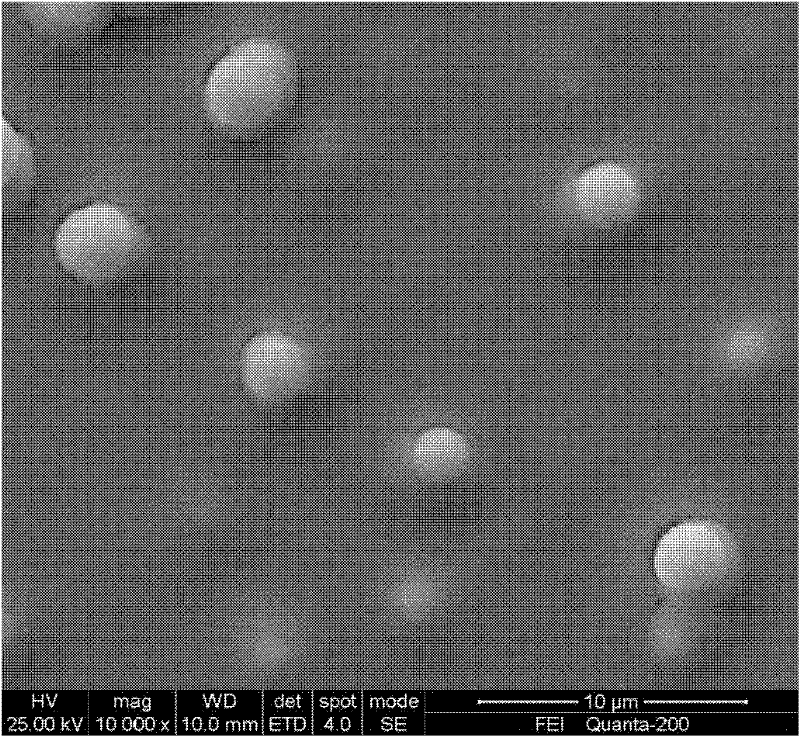
[0027] The solute composition is 0.003mol / L CuCl 2 , 0.01mol / L InCl 3 , 0.001mol / L SeO 2 , 0.1mol / L lithium chloride, 0.2mol / L trisodium citrate in 500ml aqueous solution, adjust the pH to 1.8 with dilute hydrochloric acid or sodium hydroxide; use a photoelectric cell, with FTO glass substrate as the working electrode, large area The graphite sheet was used as the counter electrode, and the saturated calomel electrode (SCE) was used as the reference electrode; the following photoelectrochemical deposition parameters were used: the incident light was a 500W xenon lamp light source (the light intensity was 10000mW cm -2 ) xenon lamp light source, working electrode potential -0.6V (vs SCE); deposit CuIn containing copper, indium and selenium with a thickness of 0.1 to 2 microns on the cathode substrate 1~2 Se 1~4 Thin films; the electrolyte temperature was 20°C, and the deposition time was 40 minutes. After testing, the obtained CuIn 1~2 Se 1~4 Film band gap E g =1.0eV, th...

Embodiment 3

[0035] The trisodium citrate in Example 2 is replaced by potassium cyanide or potassium pyrophosphate or nitrilotriacetic acid, the deposition potential is adjusted to 1.5V (vs SCE), and other conditions remain unchanged, finally CuIn with better morphology can be obtained 1~2 Se 1~4 Semiconductor thin film materials. After testing, the obtained CuIn 1~2 Se 1~4 Film band gap E g =1.1eV, the absorption coefficient is 10 5 cm -1 , the resistivity is 7.0Ωcm, and the carrier concentration is 7.9×10 18 cm -3 .


PUM

PropertyMeasurementUnit
Bandgap widthaaaaaaaaaa
Absorption coefficientaaaaaaaaaa
Resistivityaaaaaaaaaa

Abstract

The invention relates to a method for preparing a copper indium gallium selenide film by photoelectrochemical deposition, which is to deposit a copper indium gallium selenide film on a substrate placed in an electrolyte by using a photoelectrochemical deposition method; the electrolyte is selected from aqueous solution, organic solution, ion Liquid or mixed solution, which contains at least one of copper, indium, gallium, and selenium ions; the photoelectrochemical deposition process parameters are: the working electrode potential is -6.0 ~ 1.5V (vs SCE); at least one single color The light is used as incident light, and the included angle between the incident direction of the incident light and the working electrode is 0-90°. Finally, heat treatment can be performed on the obtained film. The invention solves the problems of poor film morphology, difficulty in indium and gallium deposition, and slow film growth rate encountered in traditional electrodeposited copper indium gallium selenide films, and has the advantages of good film quality, fast growth rate, controllable composition and good shape etc., the preparation method is low in cost, easy to realize large-area deposition of copper indium gallium selenide thin film, and is conducive to its large-scale industrial promotion and application.

Description

technical field [0001] The invention relates to a preparation method of a copper indium gallium selenium thin film solar cell absorbing layer material, in particular to a preparation method of photoelectrochemical deposition of a copper indium gallium selenide thin film, which belongs to the technical field of solar cell preparation. Background technique [0002] CuInSe 2 (CIS) thin film solar cells have become one of the most important and most promising solar cells. CuInSe 2 The thin film is a direct energy gap semiconductor material with an energy gap of 1.05eV, and can be formed by doping Ga to form copper indium gallium selenide Cu(In,Ga)Se 2 (CIGS) continuously adjusts the energy gap width within 1.05-1.67eV, which is suitable for the photoelectric conversion requirements of sunlight; copper indium gallium selenide (CIGS) thin film has a high light absorption coefficient (up to 10 5 cm -1 ), and stable performance, no light attenuation effect, so it has been widely...

Claims


Application Information

Patent Timeline
IPC IPC(8): C25D3/56C25D5/48
Inventor 赖延清刘芳洋杨佳贾明李劼刘业翔
Owner CENT SOUTH UNIV
Why Eureka
Try Eureka