

Seed crystal layer-assisting surface texturing zinc oxide transparent conductive film and preparation method thereof
A technology of transparent conductive film and surface texture, which is applied in chemical instruments and methods, coatings, crystal growth, etc., can solve problems such as complex process, affecting solar cell performance, film polycrystalline boundaries, dislocations, etc., so that no follow-up Effects of acid corrosion, good industrialization prospects, and good film properties
- Summary
- Abstract
- Description
- Claims
- Application Information
AI Technical Summary
Problems solved by technology
Method used
Image

Examples
Embodiment 1
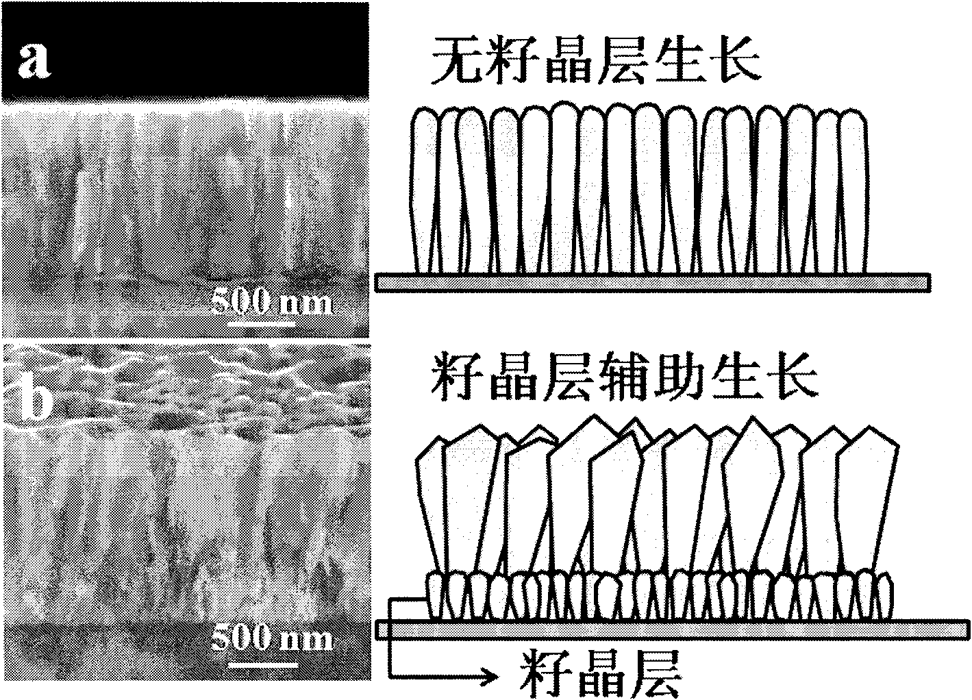
[0071] Ordinary glass is used as the substrate, and the ZnO:Al seed layer is prepared by magnetron sputtering on it, and the ZnO-based doping compound (ZnO:Al) is used as the target material, and the doping ratio of Al is 2.0 of that of Zn element. mol%, background vacuum pumped to 3.0×10 -4 Pa, using argon with a purity of 99.99% as the working gas, the working pressure is maintained at 1.2Pa, room temperature sputtering is used, the distance between the target and the substrate is set to 7cm, DC magnetron sputtering is used, the sputtering power is 60W, and the deposition The time is 10 min, and the deposited seed layer grows along the preferred orientation of (002) crystal plane, with a thickness of 200 nm. Then, the seed layer is used as the initial crystal nucleus, and a ZnO:Al thin film is deposited on it by magnetron sputtering. Using ZnO-based doping compound (ZnO:Al) as the target material, the doping ratio of Al is 2.0mol%, and the background vacuum is pumped to 3.0...
Embodiment 2
[0074] Using ordinary glass as the substrate, the seed layer of ZnO:Al is first prepared by magnetron sputtering method, and the ZnO-based doping compound (ZnO:Al) is used as the target material, and the doping ratio of Al is 1.0mol% of Zn element , background vacuum to 3.0×10 -4 Pa, with argon with a purity of 99.99% as the working gas, the working pressure is maintained at 2.0Pa, room temperature sputtering is used, the distance between the target and the substrate is set to 7cm, DC magnetron sputtering is used, the sputtering power is 50W, and the deposition The time is 5 minutes, and the deposited seed layer grows along the preferred orientation of the (002) crystal plane, with a thickness of 80 nm. Then, the seed layer is used as the initial crystal nucleus, and a ZnO:Al thin film is deposited on it by magnetron sputtering. Using ZnO-based doping compound (ZnO:Al) as the target material, the doping ratio of Al is 2.0mol% of the Zn element, and the background vacuum is pu...
Embodiment 3
[0081] Using ordinary glass as the substrate, Zn(CH 3 COO) 2 2H 2 O and Ti(OR) 4 As a raw material, the doping ratio of Ti is 1.5mol% of the Zn element, and the film obtained by the sol-gel method is subjected to an annealing temperature of 550 ° C for 30 minutes to obtain a ZnO:Ti seed layer, and the prepared seed layer is along ( 002) crystal face preferred orientation growth, the thickness is 20nm. Then, the seed layer is used as the initial crystal nucleus, and the ZnO:Ti thin film is deposited on it by magnetron sputtering. Using ZnO-based doping compound (ZnO:Ti) as the target material, the doping ratio of Ti is 5.0mol%, and the background vacuum is pumped to 3.0×10 -4 Pa, with argon with a purity of 99.99% as the working gas, and a small amount of O 2 and H 2 Gas (O 2 and H 2 accounted for 5% and 2% of the total gas flow respectively), the working pressure was maintained at 1.2Pa, the substrate temperature was 90°C, the distance between the target and the substr...
PUM
| Property | Measurement | Unit |
|---|---|---|
| thickness | aaaaa | aaaaa |
| thickness | aaaaa | aaaaa |
| length | aaaaa | aaaaa |
Abstract
Description
Claims
Application Information