

Solar cell and preparation method thereof
A technology of solar cells and conductive layers, applied in the field of solar cells, can solve the problems of low short-circuit current, low photoelectric conversion efficiency, low carrier mobility, etc. Photoelectric conversion efficiency, the effect of improving transmission efficiency
- Summary
- Abstract
- Description
- Claims
- Application Information
AI Technical Summary
Problems solved by technology
Method used
Image


Examples
preparation example Construction
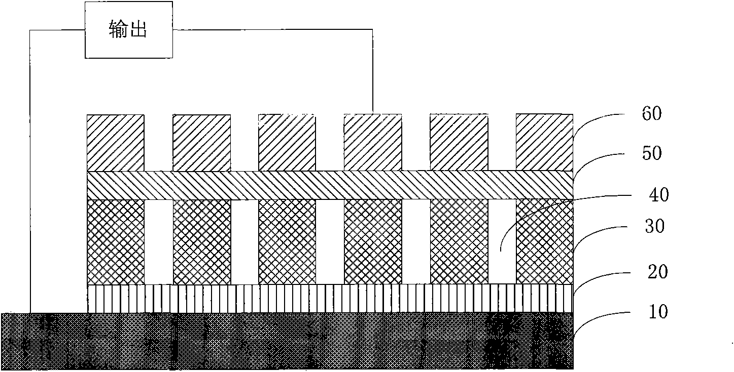
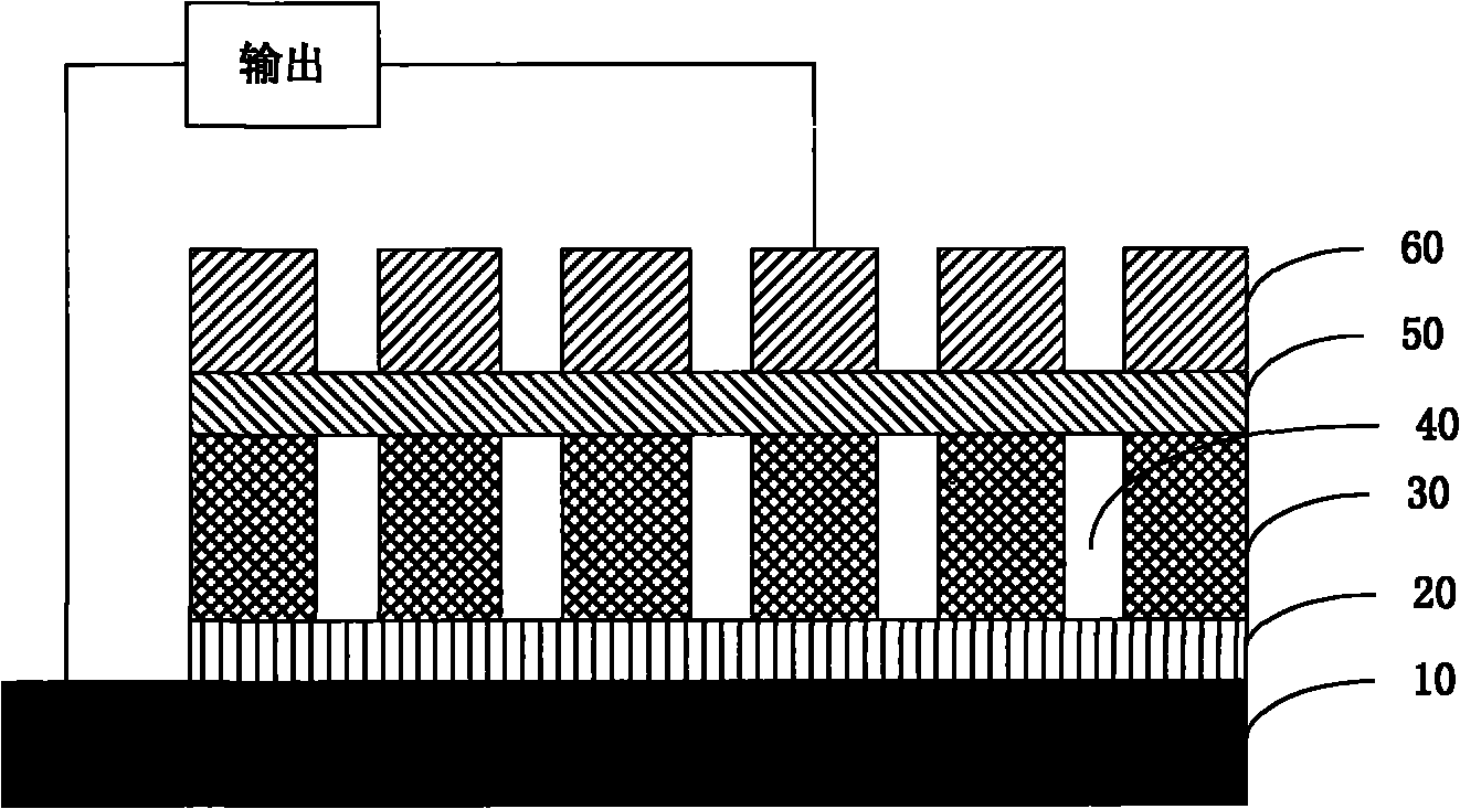
[0039] The solar cell of above-mentioned structure, its preparation method comprises the following steps:
[0040] (1) Clean the substrate to make the surface of the substrate clean and increase its surface adhesion;
[0041] (2) Deposit a certain thickness of conductive electrodes on the back of the above-mentioned substrate, but not limited to using methods such as vacuum evaporation, magnetron sputtering, chemical vapor deposition, etc., to deposit a certain thickness of conductive electrodes on the back of the above-mentioned substrate. Metals such as aluminum, magnesium, gold, silver and their alloys are then annealed in a protective atmosphere to form ohmic contact electrodes;
[0042] (3) In a vacuum chamber, semiconductor nanopillar arrays can be prepared on the above substrate by methods such as chemical vapor deposition, inductively coupled plasma etching, electron beam exposure, electron beam evaporation, and low-temperature vacuum sputtering;
[0043] (4) Vacuum c...
Embodiment 1
[0049] (1) the ZnO substrate is 0.5% H in the mass percentage concentration 2 o 2 Soak in the mixed solution with ammonia water for 5 minutes, then ultrasonic treatment for 10 minutes, wash with deionized water and dry for later use;
[0050] (2) Deposit 10 μm thick metal copper on the back of the substrate by chemical vapor deposition, and then perform annealing treatment at 450° C. for 40 minutes under a protective atmosphere to form a metal copper electrode with ohmic contact;
[0051] (3) In a vacuum chamber, electron beam evaporation is used to prepare In-Zn-O nanocolumn arrays on the ZnO substrate material. The average diameter of the nanocolumns is 100nm, the height is 1000nm, and the spacing between the columns is 100nm;
[0052] (4) Prepare a chlorobenzene solution with a mass ratio of P3HT and PCBM of 4:1, uniform mixing, and a total concentration of 15 mg / ml, fill the mixed solution into the gap formed by the semiconductor nanopillar array, and dry it after self-as...
Embodiment 2
[0057] (1) The AlN substrate was mixed with 0.5% H 2 o 2 Soak in the mixed solution with ammonia water for 5 minutes, then ultrasonic treatment for 10 minutes, wash with deionized water and dry for later use;
[0058] (2) Deposit metal aluminum with a thickness of 5 μm on the back surface of the substrate by vacuum evaporation, and then perform annealing treatment at 350° C. for 20 minutes under a protective atmosphere to form an ohmic-contact metal aluminum electrode;
[0059] (3) In a vacuum chamber, the self-chemical vapor deposition method is used to prepare an array of AlN material nanocolumns on an AlN substrate. The average diameter of the nanocolumns is 30nm, the height is 100nm, and the spacing between the columns is 30nm;
[0060] (4) Using the vacuum co-evaporation method, 4G1-3S and PCBM are filled in the gap formed by the semiconductor nanocolumn array at a mass ratio of 1:1, and then plasma treatment is performed to make the organic material and the semiconducto...
PUM
| Property | Measurement | Unit |
|---|---|---|
| Thickness | aaaaa | aaaaa |
| Thickness | aaaaa | aaaaa |
| Width | aaaaa | aaaaa |
Abstract
Description
Claims
Application Information