Method for enhancing luminous efficiency of multiquantum well of semiconductor diode

A technology of multiple quantum wells and luminous efficiency, applied in semiconductor devices, electrical components, circuits, etc., can solve the problem of reducing the luminous efficiency of quantum wells, and achieve the effect of improving the probability of crossing, uniform distribution, and preventing the decline of efficiency.

Active Publication Date: 2012-03-07
HC SEMITEK ZHEJIANG CO LTD
View PDF6 Cites 43 Cited by
  • Summary
  • Abstract
  • Description
  • Claims
  • Application Information

AI Technical Summary

Problems solved by technology

[0008] The purpose of the present invention is to provide a GaN-based multi-quantum well for the problem of the huge built-in electric field existing in the GaN-based light-emitting diode produced in the prior art and the problem of the quantum well luminous efficiency reduction caused by the uneven distribution of carriers. Fabrication method of structured blue-green light-emitting diode

Method used


Image

  • Method for enhancing luminous efficiency of multiquantum well of semiconductor diode
  • Method for enhancing luminous efficiency of multiquantum well of semiconductor diode
  • Method for enhancing luminous efficiency of multiquantum well of semiconductor diode

Examples


Embodiment 1

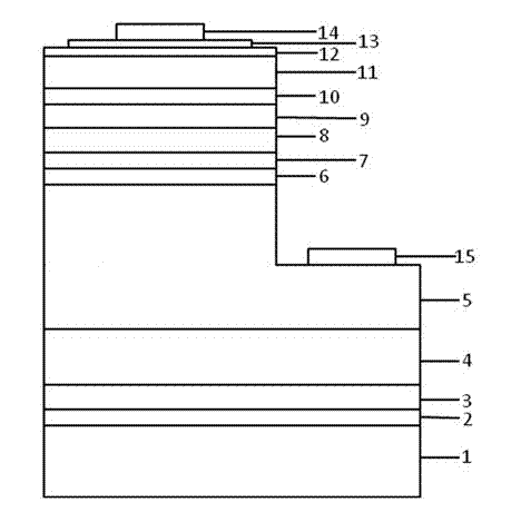
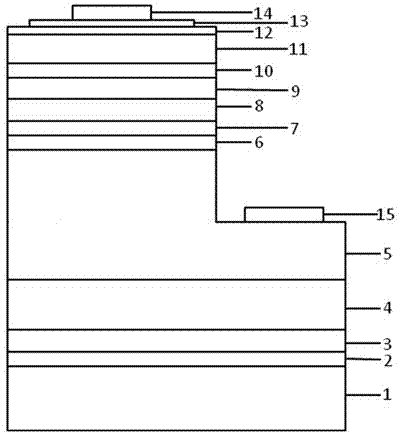
[0034] Such as figure 1 Shown:

[0035] (1) Substrate 1: First, anneal the sapphire substrate at a temperature of 1200°C in a pure hydrogen atmosphere, and then lower the temperature to 600°C for nitriding treatment;

[0036] (2) Low-temperature buffer layer 2: grow a 20nm-thick low-temperature GaN nucleation layer at 600°C. During this growth process, the growth pressure is 420Torr, and the V / III molar ratio is 900;

[0037] (3) High-temperature buffer layer 3: After the growth of low-temperature buffer layer 2 is completed, stop feeding TMGa, raise the substrate temperature by 1220°C, and anneal the low-temperature buffer layer 2 in situ, and the annealing time is 8 minutes; after annealing , adjust the temperature to 1220°C, and epitaxially grow high-temperature undoped GaN with a thickness of 1.2 μm under the lower V / III molar ratio. During this growth process, the growth pressure is 200 Torr, and the V / III molar ratio is 1500 ;

[0038] (4) N-type layer 4: After the...

Embodiment 2

[0053] In Example 2, the growth methods of the epitaxial layers 1, 2, 3, 4, 5, 6, 7, 9, 10, 11, and 12 are the same as those in Example 1. The difference lies in the growth method of the multi-quantum well layer 8: the growth temperature of the well region in MQW (8) is 880°C, 860°C, 840°C, 820°C, and 800°C in sequence, and the In Composition, the flow rate of In during the growth process remains unchanged, and the composition of In is 0.04, 0.08, 0.12, 0.16, 0.20;

[0054] After the chip manufacturing process and testing under the same conditions, the optical output power of a 10×8mil single small chip is 5.4mW, the working voltage is 3.18V, and it can be antistatic: the human body model is 5000V.

Embodiment 3

[0056] In Example 3, the growth methods of the epitaxial layers 1, 2, 3, 4, 5, 6, 7, 9, 10, 11, and 12 are the same as those in Example 1. The difference lies in the growth method of the multi-quantum well layer 8: the growth temperature of the barrier region in the MQW (8) is 950°C, 940°C, 930°C, 920°C, and 910°C in sequence, and the flow rate of In in the well region is kept constant. The change of the temperature of the barrier region changes the In composition of the well region, and the composition of In is 0.06, 0.12, 0.18, 0.24, 0.3 in turn;

[0057] After the chip manufacturing process and testing under the same conditions, the optical output power of a 10×8mil single small chip is 5.5mW, the working voltage is 3.23V, and it can be antistatic: the human body model is 5000V.


PUM


Abstract

The invention discloses a method for enhancing the luminous efficiency of a multiquantum well of a semiconductor diode. A novel gradient growth method is adopted as a multiquantum well growth manner of an epitaxial wafer structure of a light emitting diode; in the multiquantum well structure, InGaN components in the first several periods are gradually increased, so that the stress generated in the growth process of suddenly transferring GaN to InGaN with high In components is eased, and thus the polarization effect is reduced, the crystal quality of the quantum well is improved, and the compounding possibility is increased. In addition, the thicknesses of barrier layers in the first several periods are gradually reduced, the speed of electrons and the traversing possibility of electrons can be reduced by the barrier layers with larger thickness, the traversing possibility of electron holes can be increased by the barrier layers with smaller thickness, so that the electrons and the electron holes are distributed more uniformly and the problem of the reduced efficiency under high current injection is avoided, and therefore the luminous efficiency of the multiquantum well is improved.

Description

technical field [0001] The invention relates to a new method which can be applied to semiconductor light-emitting diodes, especially gallium nitride-based blue-green light-emitting diodes, and can effectively improve the luminous efficiency of its multi-quantum wells. Background technique [0002] Represented by gallium nitride (GaN) The group nitride is a wide bandgap semiconductor material with a direct band gap, which has high electron drift saturation velocity, good thermal conductivity, radiation resistance, high temperature resistance, and good chemical and physical stability. Its ternary alloy indium gallium nitride (InGaN) band gap is continuously adjustable from 0.7eV indium nitrogen (InN) to 3.4eVGaN, so that its emission wavelength covers the entire region of visible light and near ultraviolet light. The blue-green light-emitting diode (LED) with InGaN / GaN multiple quantum wells as the active layer has remarkable features such as high efficiency, environmental p...

Claims


Application Information

Patent Timeline
Patent Type & Authority Applications(China)
IPC IPC(8): H01L33/00
Inventor 吴克敏魏世祯董彬忠王江波
Owner HC SEMITEK ZHEJIANG CO LTD
Why Eureka
Try Eureka