Amorphous indium zinc oxide/carbon nanotube composite film transistor and preparation method thereof

A carbon nanotube composite and thin-film transistor technology, which is applied in the direction of transistors, semiconductor/solid-state device manufacturing, semiconductor devices, etc., can solve the problems of large-area preparation of high-mobility polysilicon materials, large off-state current of TFT, and gap in flexibility. , to achieve excellent mechanical stability, high mobility, and low cost

Inactive Publication Date: 2012-03-28
WUHAN UNIV
View PDF2 Cites 15 Cited by
  • Summary
  • Abstract
  • Description
  • Claims
  • Application Information

AI Technical Summary

Problems solved by technology

However, currently p -Si-based TFT has two problems: one is that the off-state current of TFT is relatively large; the other is that it is difficult to prepare high-mobility polysilicon materials in a large area at low temperature
[0008] However, it takes a process f

Method used


Image

  • Amorphous indium zinc oxide/carbon nanotube composite film transistor and preparation method thereof
  • Amorphous indium zinc oxide/carbon nanotube composite film transistor and preparation method thereof
  • Amorphous indium zinc oxide/carbon nanotube composite film transistor and preparation method thereof

Examples


Embodiment 1

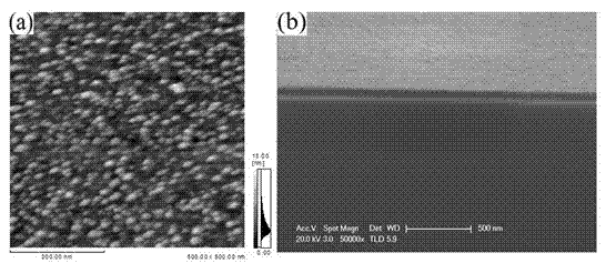
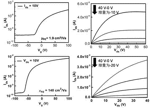
[0029] (1) Dissolve 0.285 g of indium nitrate tetrahydrate and 0.165 g of zinc acetate dihydrate in 50 mL of ethylene glycol methyl ether, and add 0.46 mL of ethanolamine as a stabilizer, stir for 2 h, and have a thickness of 300 nm for pre-grown SiO 2 The highly doped Si sheet of the insulating layer was ultrasonically cleaned, and then spin-coated with a spin coater at a speed of 2400 rpm, and then baked at 200 °C for 10 min in the atmosphere, and then spin-coated on the basis of the previous layer. layer to obtain a composite film with a thickness of 60 nm, and finally thermally annealed at 400 °C for 40 min in the atmosphere to obtain a composite film material; (2) using ultraviolet lithography technology, through the first mask, using wet etching (10 wt% dilute hydrochloric acid) for 2 min, the film was divided into small pieces with an area size of 1 mm × 1 mm to reduce the parasitic capacitance and leakage current introduced during the transistor fabrication process. T...

Embodiment 2

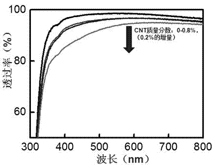
[0031] (1) Dissolve 9 mg of carbon nanotubes (CNTs) in 100 mL of ethylene glycol methyl ether by sonication, and suspend them evenly for 4 h to serve as mother liquor for later use. Then 0.285 g of indium nitrate tetrahydrate and 0.165 g of zinc acetate dihydrate were dissolved in 50 mL of ethylene glycol methyl ether, and 0.46 mL of ethanolamine was added as a stabilizer, stirred for 2 h, and 50 mL of carbon nanotube mother liquor was added and ultrasonicated Disperse for 30 min, and then spin-coat at 2400 rpm on pre-grown SiO with a thickness of 300 nm 2 On the insulating layer, after baking at 200 °C for 10 min in the atmosphere, spin-coat another layer on the basis of the previous layer to obtain a composite film with a thickness of 60 nm, and finally thermally anneal at 400 °C for 40 min in the atmosphere to obtain IZO / CNT composite film material; (2) Using ultraviolet lithography technology, through the first mask, using wet etching (10 wt% dilute hydrochloric acid as e...

Embodiment 3

[0035] (1) Dissolve 9 mg of carbon nanotubes (CNTs) in 100 mL of ethylene glycol methyl ether by sonication, and suspend them evenly for 4 h to serve as mother liquor for later use. Then 0.285 g of indium nitrate tetrahydrate and 0.165 g of zinc acetate dihydrate were dissolved in 50 mL of ethylene glycol methyl ether, and 0.46 mL of ethanolamine was added as a stabilizer, stirred for 2 h, 50 mL of carbon nanotube mother liquor was added and Ultrasonic dispersion was performed for 30 min, and then spin-coated on pre-grown SiO with a thickness of 300 nm at a speed of 2400 rpm. 2 On the insulating layer, after baking at 200 °C for 10 min in the atmosphere, spin-coat another layer on the basis of the previous layer to obtain a composite film with a thickness of 60 nm, and finally thermally anneal at 300 °C for 40 min in the atmosphere to obtain IZO / CNT composite film material; (2) Using ultraviolet lithography technology, through the first mask, using wet etching (10 wt% dilute ...


PUM


Abstract

The invention provides an amorphous indium zinc oxide/carbon nanotube composite film transistor. A flexible indium zinc oxide/carbon nanotube composite film is taken as a semiconductor channel layer. In the composite film, a mass ratio of the carbon nanotube to the indium zinc oxide is between 0.027% and 2.74%. The carbon nanotube is added into an indium salt-zinc salt composite colloid solution so as to prepare a carbon nanotube/ indium salt-zinc salt composite colloid solution. A spin coating technology is used to prepare the indium zinc oxide/carbon nanotube composite film with high performance. And then through subsequent thermal annealing, photoetching, etching, photoetching, evaporation and stripping of an electrode, an indium zinc oxide/carbon nanotube composite film field effect transistor with high mobility can be prepared. Through optimizing some technologies, the indium zinc oxide/carbon nanotube with the high field effect and the mobility can be successfully prepared and the indium zinc oxide/carbon nanotube possesses a high mechanical property. Experimental costs are low. A requirement to an experiment condition is low. Repeatability of an experiment result is high. Large-scale batch production can be realized.

Description

[0001] technical field [0002] The invention relates to an amorphous indium zinc oxide / carbon nanotube composite thin film transistor and a preparation method thereof, belonging to the field of nanometer materials and nanometer devices. Background technique [0003] With the advent of the information age, display devices (LCD) and electronic paper are accelerating towards flat panelization and energy saving. Among them, active array drive display devices with thin-film transistors (TFT) as switching elements have become one of the most popular flat panel display technologies. of the best. TFT is a field-effect semiconductor device, including several important components such as substrate, semiconductor channel layer, insulating layer, gate and source-drain electrodes, among which the semiconductor channel layer is crucial to device performance. [0004] At present, for TFT-LCD, the semiconductor channel layer mainly adopts amorphous silicon ( a -Si) and polysilicon thin f...

Claims


Application Information

Patent Timeline
IPC IPC(8): H01L29/24H01L29/10H01L29/786H01L21/336
Inventor 廖蕾刘曰利刘兴强陈文贺彪
Owner WUHAN UNIV
Why Eureka
Try Eureka