Preparation method of wafer-grade spherical micro-lens array

A microlens array and wafer-level technology, which is applied in the field of preparation of new microlens arrays, can solve the problems of high manufacturing cost of metal molds and high requirements for dimensional control, and achieve the effect of improving mechanical reliability

Inactive Publication Date: 2012-06-13
SOUTHEAST UNIV
View PDF5 Cites 14 Cited by
  • Summary
  • Abstract
  • Description
  • Claims
  • Application Information

AI Technical Summary

Problems solved by technology

In these manufacturing methods, metal materials are usually used as the mold of the lens array, and because the optical microlens has high requirements for dimensional control, the manufacturing cost of the metal mold is usually very high.

Method used


Image

  • Preparation method of wafer-grade spherical micro-lens array
  • Preparation method of wafer-grade spherical micro-lens array
  • Preparation method of wafer-grade spherical micro-lens array

Examples


Embodiment 1

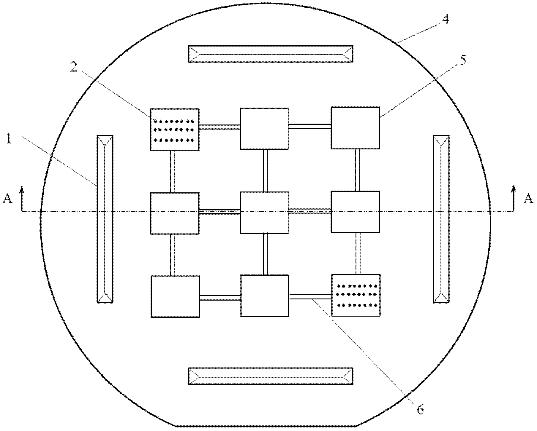
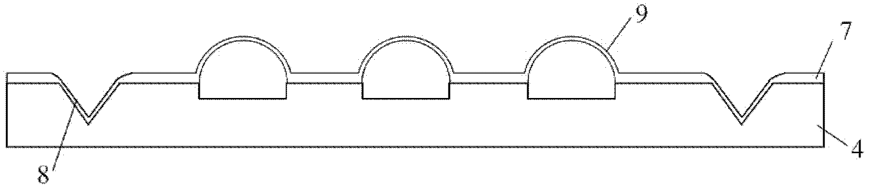
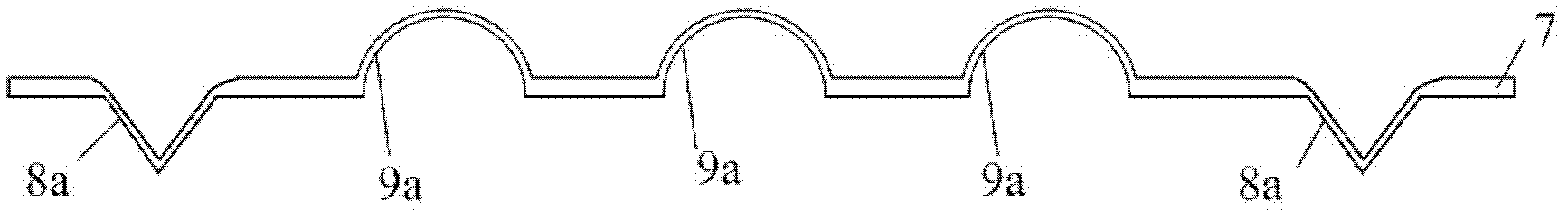
[0025]A method for preparing a wafer-level spherical microlens array, comprising the following steps: in the first step, respectively etching a lens mold microgroove array and a self-aligned silicon mold microgroove on a silicon wafer (such as a 4-inch wafer) to obtain The silicon wafer mold and the microgroove array of the lens mold are etched and connected by microchannels. The process for preparing the pattern structure on the silicon wafer is one or a combination of wet etching process, reactive ion etching (RIE) process or deep reactive ion etching (DRIE); in the second step, in the A certain amount of thermal air release agent powder is placed in the lens mold micro-groove array of the silicon wafer. The thermal air release agent is a powder that can release gas after heating, calcium carbonate powder or titanium hydride powder, and the powder particle size is 300 mesh or 800 mesh. Or 1000 mesh. The added mass is calculated according to the size of the required molding ...

Embodiment 2

[0028] A method for preparing a wafer-level spherical microlens array, comprising the following steps:

[0029] The first step: using 25% TMAH solution wet etching method to etch the shape on a 4-inch silicon wafer to form a microcavity array of a specific size.

[0030] The second step: coating a thermal air release agent in part of the microcavity array. The heat release agent is a powder that can release gas after heating, such as calcium carbonate powder or titanium hydride powder, and the particle size of the powder is 300 mesh, 800 mesh or 1000 mesh. The added mass is calculated according to the size of the required molding cavity, for example, if calcium carbonate is used, the mass can be 0.1mg, 0.5mg, 1mg, 1.5mg, 2mg.

[0031] Step 3: bonding the borosilicate glass wafer to the silicon wafer mold, so that the microcavity array of the silicon wafer mold is sealed. In the present invention, the glass is Pyrex7740 glass, the bonding is anodic bonding, and the typical pr...


PUM


Abstract

The invention discloses a mould for a spherical micro-lens array, and a preparation method thereof. The method is characterized in that the method comprises steps that: a lens mould micro-groove array and self-aligning silicon mould micro-grooves are respectively etched on a silicon wafer; micro-channels are etched among the lens mould micro-groove array, and are used for connecting the lens mould micro-grooves; a certain amount of heat-released aerosol power is placed; a borosilicate glass wafer is bonded with the silicon wafer under a vacuum condition; the bonded wafers are heated; under the effect of vacuum negative pressure, softened glass is automatically filled into the self-aligning silicon grooves, such that self-aligning glass convex blocks are obtained; the materials are cooled and annealed; silicon is removed, such that a glass mould is obtained; corresponding self-aligning grooves and mould grooves used for controlling lens spaces are etched; anti-adhesion treatments are carried out on the surfaces of the glass mould and the silicon mould; a UV curable adhesive is filled in a spherical glass micro-cavity of the glass mould, such that the lens-molding silicon wafer is self-aligned with the glass mould; the UV curable adhesive in the mould is cured, and the wafer-grade spherical micro-lens array can be obtained after demolding. The method provided by the invention is advantaged in simple technology, low cost, and good reliability.

Description

technical field [0001] The invention relates to a MOEMS (micro-opto-electromechanical system) packaging technology, in particular to a preparation method of a novel microlens array. Background technique [0002] In recent years, portable consumer electronic product terminals such as mobile phones are equipped with tiny video camera modules. The video camera module generally includes a solid-state image acquisition element such as an image sensor (CCD or CMOS image sensor), and a lens (group) that forms an image on the light-receiving surface of the solid-state image acquisition element. [0003] With the continuous miniaturization / thinning of portable electronic products, the video camera module therein should also be further miniaturized / thinning, and meet the requirements of cost-effective factors. Microlenses and their arrays have significant applications in micro-optical systems. They can be used in optical information processing, optical computing, optical interconnect...

Claims


Application Information

Patent Timeline
Patent Type & Authority Applications(China)
IPC IPC(8): B81C1/00H01L27/146
Inventor 尚金堂秦顺金于慧蒯文林
Owner SOUTHEAST UNIV
Why Eureka
Try Eureka