Method for manufacturing organic polymer optical waveguide amplifier by ultraviolet nanoimprint lithography

A technology of optical waveguide amplifier and nanoimprinting, which is applied in the direction of optical waveguide light guide, light guide, optics, etc., to achieve the effects of improving process precision and efficiency, small line width, and simple preparation process

Inactive Publication Date: 2012-07-11
JILIN UNIV
View PDF2 Cites 14 Cited by
  • Summary
  • Abstract
  • Description
  • Claims
  • Application Information

AI Technical Summary

Problems solved by technology

Nano-imprinting of UV-curable materials prepares polymer grooves, and after peeling off, directly fills erbium-doped organic

Method used


Image

  • Method for manufacturing organic polymer optical waveguide amplifier by ultraviolet nanoimprint lithography
  • Method for manufacturing organic polymer optical waveguide amplifier by ultraviolet nanoimprint lithography
  • Method for manufacturing organic polymer optical waveguide amplifier by ultraviolet nanoimprint lithography

Examples


Embodiment 1

[0045] Example 1: Si Template Nanoimprint Ridged Er 1.2 Yb 0.8 (PBa) 6 (Phen) 2 EDWA

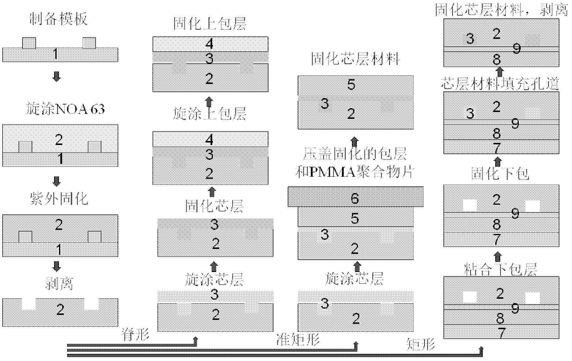
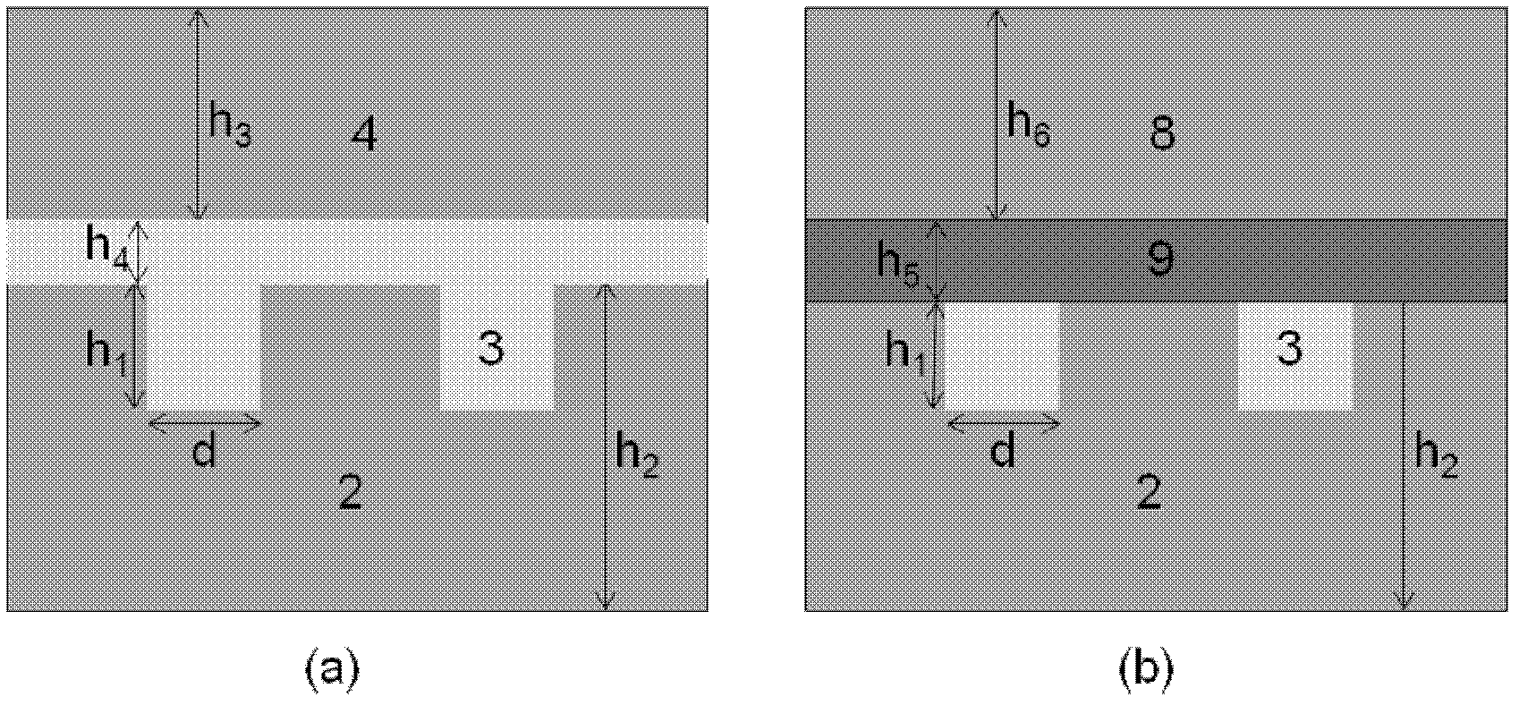
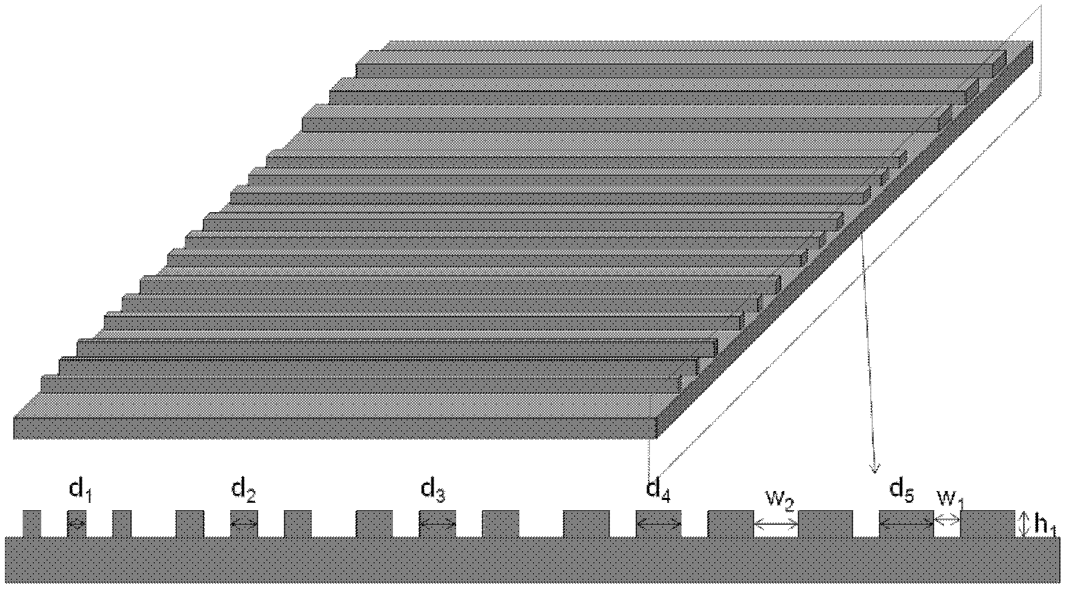
[0046] Prepare a Si template (1) with a raised waveguide pattern, the waveguide length (L) is 3cm, there are 5 groups of waveguide arrays, each group of waveguide arrays includes 3 waveguides, and the interval of each waveguide (w 1 ) is 200 microns, the width (d) of each waveguide in each group array is 1 μm, 2 μm, 4 μm, 6 μm and 8 μm respectively, the height (h1) of the waveguide is 3 microns, the spacing of the waveguide array (w 2 ) is 400 μm;

[0047] Polymer material NOA63 (without diluting toluene) is coated on the Si template (1) with the raised waveguide pattern that has been treated (wipe with acetone first, then with ethanol, and finally with deionized water), at 1500 rpm Rotate at a speed of 1 minute, and the rotation time is 30 seconds to obtain a lower cladding (2) with a thickness of 45 microns, and then peel off the lower cladding (2) from the Si template (1);

[0048] ...

Embodiment 2

[0051] Example 2: Preparation of ridge-shaped ErYb(DBM) by nanoimprinting of polymer template 3 (MA) / NOA61EDWA

[0052] After cleaning (cleaning with acetone first, then ethanol, and finally deionized water) SiO 2 Spin-coat SU-8 material on top, rotate at a speed of 3000 rpm, and spin for 30 seconds to obtain a film with a thickness of about 4.5 microns. After baking at 65°C (10 minutes) and 90°C (20 minutes) , exposed under a 150W, 365nm wavelength mercury lamp for 3 minutes, followed by post-baking at 150°C (30 minutes) to enhance the bonding force between the material and the substrate. Then spin-coat a layer of SU-8 material, rotate at a speed of 2000 rpm for 30 seconds, and obtain a film of about 6 microns. After 65°C (10 minutes), 90°C (20 minutes) before and after After baking, under the mercury lamp of 350W, 365nm wavelength, the photolithography of the plate is carried out, the exposure time is 3 minutes, and then the middle baking is carried out at 65°C (10 minutes...

Embodiment 3

[0056] Example 3: Si template imprinting quasi-rectangular ErYb(DBM) 3 (Phen) / SU-8EDWA

[0057] Prepare a Si template (1) with a raised waveguide pattern, the length (L) is 3 cm, a total of 5 waveguide arrays, the width (d) of each array is 8 μm, 6 μm, 4 μm, 2 μm and 1 μm, and the height of the waveguide (h1) is 4 microns, the pitch of the waveguide array (w 2 ) is 400 microns; each waveguide array includes 3 waveguides, and the interval of each waveguide (w 1 ) is 200 microns.

[0058] Polymer material NOA63 (without diluting toluene) is coated on the Si template (1) with raised waveguide pattern that has been treated (wiping with acetone first, then ethanol, and finally rinsed with deionized water), at 1500 rpm Spinning at a rpm of 30 sec for a 45 micron thick lower cladding (2).

[0059] Put the spin-coated lower cladding layer (2) under a 400W mercury lamp for ultraviolet curing (ultraviolet nanoimprinting), the curing distance is 30cm, and the curing time is 10 minute...


PUM

PropertyMeasurementUnit
Widthaaaaaaaaaa
Thicknessaaaaaaaaaa

Abstract

The invention belongs to the technical field of polymer optical waveguide amplifier manufacturing and particularly relates to a method for manufacturing an organic polymer flexible optical waveguide amplifier by ultraviolet nanoimprint lithography. The method includes spin coating a polymer bottomcladding material on a silicon or polymer template which is high-precision and has a projecting waveguide pattern, performing ultraviolet nanoimprint curing, spin coating a soluble complex material core material with an obtained thin film which has polymer grooves to serve as a substrate, performing vacuum drying, then spin coating a polymer topcladding material, and obtaining the polymer waveguide amplifier after ultraviolet curing. According to the organic polymer optical waveguide amplifier and the manufacturing method thereof, not only is the refractivity of the polymer core material and the polymer cladding materials easily controlled, but also thickness of each layer of materials is easily controlled. The organic polymer optical waveguide amplifier is low in cost, finished product rate is high, the accuracy is high, and the organic polymer optical waveguide amplifier is suitable for mass production.

Description

technical field [0001] The invention belongs to the technical field of polymer optical waveguide amplifier preparation, and in particular relates to a method for preparing an organic polymer flexible optical waveguide amplifier by using an ultraviolet nano-imprinting technology. Background technique [0002] Erbium-doped fiber amplifier (EDFA) is one of the most important inventions in the history of optical fiber communication. Its length is generally several meters to tens of meters, which is no problem in long-distance communication; In distance transmission, the application of EDFA has certain difficulties. At the same time, in the optical communication system, in order to ensure the transmission of optical signals, it is inevitable to use some optical devices such as multiplexer / demultiplexer, beam splitter and optical switch. Compensation will greatly reduce the transmission distance of the signal, so the signal must be amplified and enhanced. In the optical communic...

Claims


Application Information

Patent Timeline
IPC IPC(8): G02B6/138G02B6/13
Inventor 衣云骥张大明王菲王旗孙小强陈长鸣
Owner JILIN UNIV
Why Eureka
Try Eureka