Diffusion method for polycrystalline silicon solar photovoltaic cell silicon chip
A technology of silicon wafers and diffusion methods for photovoltaic cells, applied in the directions of diffusion/doping, chemical instruments and methods, circuits, etc., can solve the problem of high carrier recombination rate, reduction of primary yield of silicon wafers, and reduction of minority carrier lifetime of polycrystalline silicon wafers, etc. problems, to achieve the effect of strengthening controllability, improving photoelectric conversion efficiency, and improving primary yield
- Summary
- Abstract
- Description
- Claims
- Application Information
AI Technical Summary
Problems solved by technology
Method used
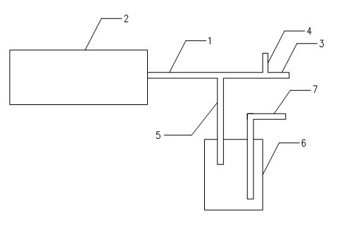
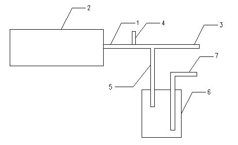
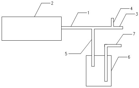
Image

Examples
Embodiment 1
[0064] Use P-type 156×156 polysilicon wafers, after cleaning the surface with hydrofluoric acid or nitric acid and making texture, put them into a tubular diffusion furnace for diffusion. The specific parameters of each step of diffusion are as follows:
[0065] Step 1, put into the furnace
[0066] The feeding speed of silicon carbide slurry is 300mm / min, the initial temperature in the tubular diffusion furnace is 800°C, and the flow rate of oxygen is 0.3L / min;
[0067] Step 2. Oxidation
[0068] The tubular diffusion furnace is heated to 835°C, the heating rate is 5°C / min, the flow rate of oxygen is 0.5L / min, and the oxidation time is 40min;
[0069] Step 3, the first phosphorus source diffusion
[0070] The temperature of the tubular diffusion furnace was adjusted to 835 °C, and the small nitrogen flow rate was 0.92L / min , the oxygen flow rate is 0.5L / min, the maximum nitrogen flow rate is 9.5 L / min, and the time for the first phosphorus source diffusion is 6min;
[00...
PUM
 Abstract
Description
Claims
Application Information