

Preparation method of N-trap high-voltage gate driving chip for directly driving power device
A technology for power devices and driver chips, which is applied in semiconductor/solid-state device manufacturing, electrical components, circuits, etc. It can solve problems such as failure to meet design, large leakage current, and complicated procedures, and achieve manufacturing cost savings, changing electric field distribution, The effect of obvious economic benefits
- Summary
- Abstract
- Description
- Claims
- Application Information
AI Technical Summary
Problems solved by technology
Method used
Image

Examples
Embodiment 1
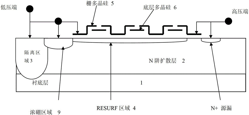
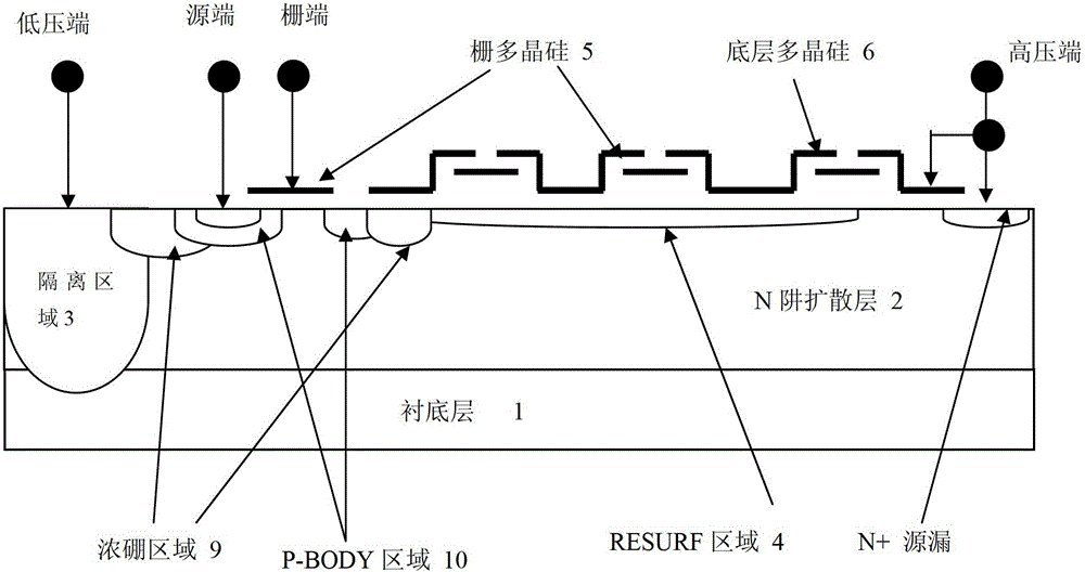
[0045] The present invention proposes a method for preparing an N-well high-voltage gate drive chip for directly driving power devices. It combines the high-voltage process with the conventional CMOS process. On the basis of using a conventional PN junction isolation, the injection Doping boron ions forms a P-type reduced surface electric field (RESURF) region on the N-well diffusion layer, and at the same time uses two layers of polysilicon (i.e. bottom polysilicon and gate polysilicon) on the surface of the PN junction to form a series of capacitive voltage dividers, such as figure 1 As shown, when the circuit is connected, the lower plate of the outermost capacitive voltage divider is grounded, and the upper plate of the innermost capacitive voltage divider is connected to a high potential, which effectively changes the surface electric field of the PN junction and changes the PN junction The direction of the electric force lines on the surface helps to reduce the electric f...
Embodiment 2
[0072] This embodiment is basically the same as Embodiment 1, and the preparation process of this embodiment is specifically as follows:
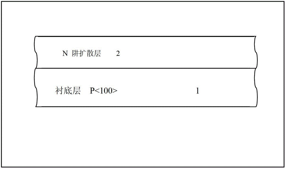
[0073] ① Select a P-type silicon wafer with a crystal orientation of (100) and a resistivity of 70ohm·cm. image 3 shown.
[0074] Here, in order to increase the threshold value of the parasitic CMOS transistor and reduce the latch-up effect of the CMOS transistor, the junction depth and concentration of the N-well diffusion layer 2 are fully considered during preparation, so in this embodiment, the junction depth of the N-well diffusion layer 2 is designed to be 13.5 μm, the sheet resistance of the N-well diffusion layer 2 is designed to be 1.2KΩ / □.
[0075] ②The P-type isolation area is prepared by high-voltage junction isolation process (HVJI), such as Figure 4 The specific process is as follows:
[0076] ②-1, growing a layer of silicon dioxide with a thickness of 730nm on the N well diffusion layer 2, and then coating a layer of pho...
Embodiment 3
[0092] The preparation method of the N-well high-voltage gate driver chip in this embodiment is basically the same as the preparation methods given in Embodiment 1 and Embodiment 2, the only difference is that in step ① of this embodiment, the crystal orientation is selected as (100) A P-type silicon wafer with a resistivity of 60ohm cm. is used as the substrate layer 1; the thickness of the silicon dioxide grown on the N well diffusion layer 2 in step ②-1 is 660nm; The thickness of the silicon dioxide grown on the region 11 and the RESURF region 4 is 90nm; the boron ions B implanted into the P well region 11 in step ③-3 11 + at a dose of 3.00E13ions / cm 2 And the energy is 80Kev; the thickness of the silicon dioxide grown on the P well region 11 and the RESURF region 4 in step ③-5 is 1400nm; the thickness of the silicon dioxide grown on the boron-rich region 9 in step ④-3 It is 90nm; In step ④-5, in the oxidation furnace, the advancing time of boron-concentrated region 9 is 5...
PUM
| Property | Measurement | Unit |
|---|---|---|
| Thickness | aaaaa | aaaaa |
| Sheet resistance | aaaaa | aaaaa |
| Pressure value | aaaaa | aaaaa |
Abstract
Description
Claims
Application Information