Flexible CdTe thin-film solar cell and preparation method thereof
A technology for solar cells and flexible cells, applied in circuits, photovoltaic power generation, electrical components, etc., can solve the problem that CdTe/CdS interfacial diffusion cannot be effectively controlled, CdTe grain defects cannot be effectively reduced, and CdTe back contacts cannot be effectively prepared and other issues, to achieve the effect of strong radiation resistance, easy mass production, and resistance to cosmic ray radiation
- Summary
- Abstract
- Description
- Claims
- Application Information
AI Technical Summary
Problems solved by technology
Method used
Image
Examples
Embodiment 1
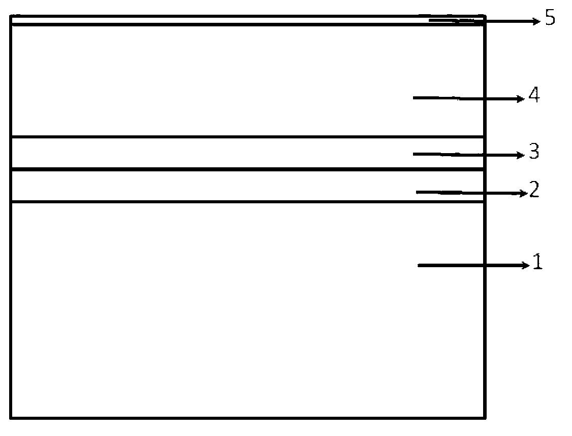
[0034] Using 1mm thick, 15×5cm fluorophlogopite as the substrate, the mica substrate 1 was cleaned, ultrasonically cleaned with acetone, ethanol and deionized water for 5 minutes each, and then cleaned with V(H 2 SO 4 ): V(H 3 PO 4 )=3:1 mixed solution was washed at 160°C for 15 minutes, finally washed with deionized water, and dried with high-purity nitrogen. Then grow a 100nm-thick AZO transparent conductive film 2 on the mica substrate by molecular beam epitaxy. The growth process is as follows: the purity of Zn, Al, and oxygen is 5N grade, and the oxygen atoms required for the reaction are generated by a 13.56MHz radio frequency plasma generator. During growth, the base pressures of the growth chamber and the pre-growth chamber were maintained at 9 × 10 -8 Pa and 5×10 -8 Pa. Before growth, transfer the substrate into the pre-growth chamber for high-temperature degassing treatment at 800°C for 30 minutes, after cooling, transfer it to the growth chamber for oxygen ato...
Embodiment 2
[0036] Fluoropheophlogite mica with a thickness of 1 mm and a size of 15×5 cm is used as the substrate 1 , the mica substrate 1 is cleaned, and then a transparent conductive film graphene 2 with a thickness of 0.3 nm is grown on the mica substrate. The graphene growth method is as follows: prepare graphene in a tube furnace by chemical vapor deposition, put a 0.5 mm thick Cu foil into the tube furnace, then heat the tube furnace to 1000 ° C, and feed methane and hydrogen, Keep at 1000°C for 15 minutes to obtain the desired graphene. Then the graphene is transferred to polymethyl methacrylate (PMMA) by a solution of ferric chloride and hydrochloric acid, and the graphene is placed on the CdTe polycrystalline film 4, and the polymethyl methacrylate is dissolved by acetone , to obtain a transparent conductive film 2 on the mica substrate 1 . Then prepare the CdS film 3 by the chemical water bath method (CBD), put the mica substrate 1 with the graphene conductive film 2 into the ...
Embodiment 3
[0038] Fluoropheophlogite mica with a thickness of 1mm and 15×5cm was used as the substrate 1. The mica substrate 1 was cleaned, and then NiO was prepared on the mica substrate by sol-gel method, and then a 500nm-thick NiO transparent conductive film 2 was grown by electron beam. The preparation process is as follows: the NiCl 3 ·6H 2 O was placed in deionized water, and then heated at 100 °C until the deionized water was completely volatilized, and then the remaining material was put into a muffle furnace and treated at 800 °C for 24 h to obtain NiO powder. Then, a 500nm thick NiO transparent conductive film 2 is prepared on the mica substrate by electron beam. Then grow the CdS thin film 3, put the mica substrate 1 deposited with the transparent conductive thin film 2 into another magnetron sputtering equipment, evacuate the chamber, and heat the substrate to 250°C at the same time, when the vacuum on the back reaches 10 -3 Below Pa, start to sputter the CdS polycrystallin...
PUM
| Property | Measurement | Unit |
|---|---|---|
| Thickness | aaaaa | aaaaa |
Abstract
Description
Claims
Application Information
