
Nanometer ceramic solar film

A nano-ceramic and solar film technology, applied in the direction of ion implantation plating, coating, layered products, etc., can solve the problems of easy oxidation of the metal layer, low visible light transmittance, low clarity and reflection, and achieve energy saving and Environmental protection, good spectral selectivity, and long service life

Inactive Publication Date: 2012-12-26
SOUTHWESTERN INST OF PHYSICS
View PDF4 Cites 11 Cited by
  • Summary
  • Abstract
  • Description
  • Claims
  • Application Information

AI Technical Summary

Problems solved by technology

The second generation is the dyed film in the 1960s. By adding pigments, films of different colors can be obtained, but they have no heat insulation effect, low visible light transmittance, poor clarity, and easy to fade.
The third generation is the vacuum evaporation film in the early 1990s. Aluminum is evaporated on the substrate to achieve heat insulation effect, but the visible light transmission is low and the reflection is high, which affects the comfort of vision.
The fourth generation is the metal magnetron sputtering film in the late 1990s, which uniformly deposits nickel, silver, titanium, gold and other metal materials on the PET substrate, which has good heat insulation effect, high definition, Low reflection and other characteristics, but there are disadvantages such as the metal layer is easy to oxidize, and it will block the signals of GPS and other in-vehicle wireless communication systems.

Method used


Image

  • Nanometer ceramic solar film
  • Nanometer ceramic solar film
  • Nanometer ceramic solar film

Examples


Embodiment Construction

[0017] The present invention will be described in further detail below in conjunction with the accompanying drawings and embodiments.

[0018] Substrate PET: polyethylene terephthalate, English name: polyethylene terephthalate. The thickness is 23μm~50μm, the transmittance is greater than 86%, and the heat resistance temperature is ≥150℃.

[0019] The first layer of titanium dioxide film: It is plated by intermediate frequency reactive magnetron sputtering twin targets, the target material is titanium target, the reaction gas is oxygen, and the film thickness is 26nm~38nm. Among them, the reactive sputtering state is monitored by the plasma emission spectrum monitoring and control device PEM, which avoids target poisoning and sparking, and improves the deposition rate and film quality.

[0020] The second layer of titanium nitride film: It is plated by twin targets of intermediate frequency reaction magnetron sputtering. The target material is titanium target, the reaction ga...


PUM

PropertyMeasurementUnit
thicknessaaaaaaaaaa
thicknessaaaaaaaaaa
thicknessaaaaaaaaaa

Abstract

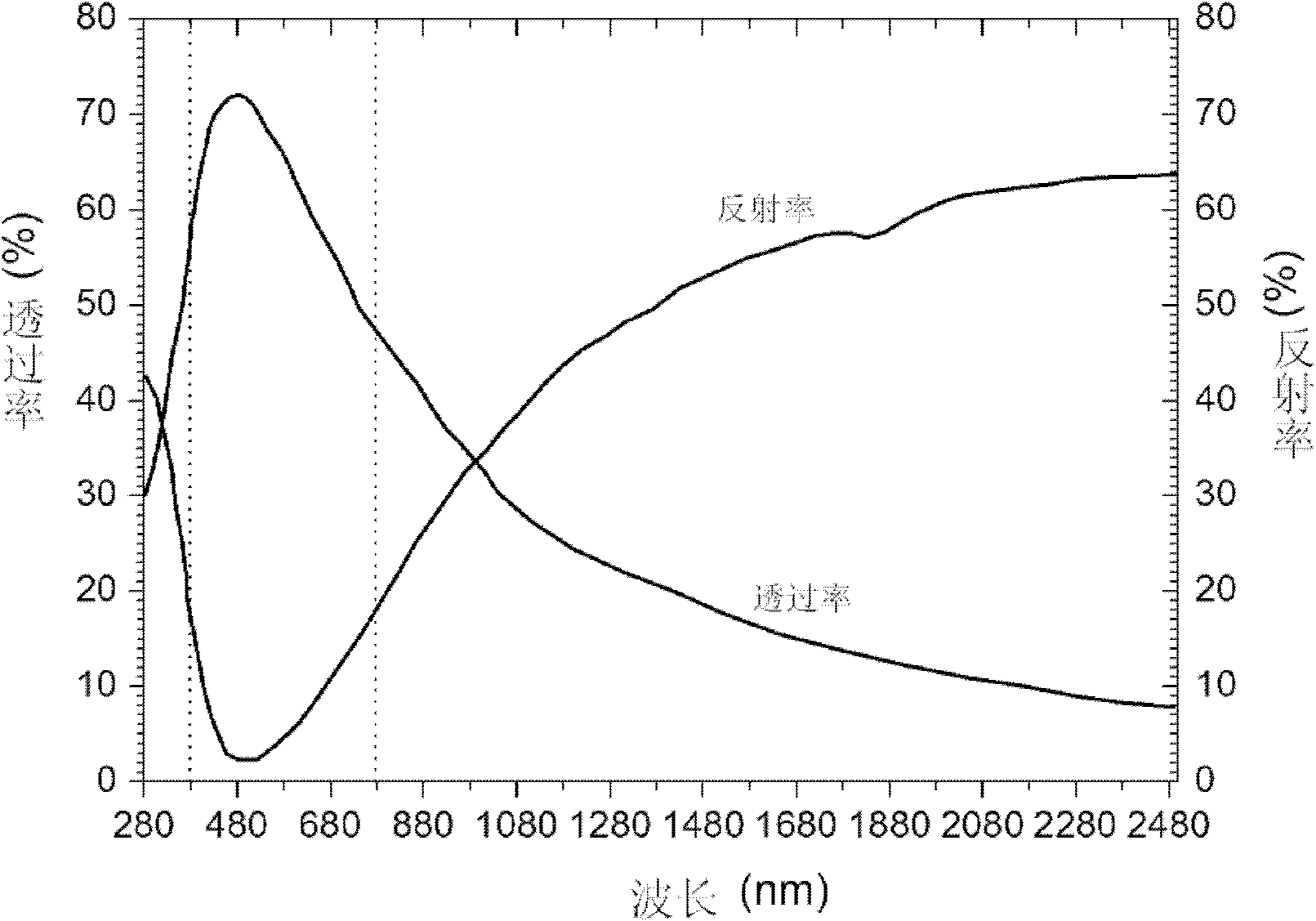
The present invention relates to a nanometer ceramic solar film. According to the nanometer ceramic solar film, a firs layer titanium dioxide film, a second layer titanium nitride film and a third titanium dioxide film are sequentially plated on a surface of a substrate PET through magnetron sputtering, wherein a thickness of the substrate PET is 23-50 mum, a thickness of the first layer titanium dioxide film is 26-38 nm, a thickness of the second layer titanium nitride film is 20-26 nm, and a thickness of the third layer titanium dioxide film is 26-38 nm. The nanometer ceramic solar film of the present invention has the following characteristics that: good spectral selective permeability, high transmittance in a visible light region, and high reflectivity in an infrared region are provided, wherein infrared rays are blocked so as to reduce heat source, such that thermal insulation is achieved while transmittance on visible light is not affected; and titanium dioxide and titanium nitride have high chemical stability at a room temperature, are not easily oxidized, and do not react with oxygen, water, steam, hydrochloric acid, sulfuric acid and the like under normal circumstances, such that performances are stable, fading and discoloration can not be generated, and a service life is long.

Description

technical field [0001] The invention relates to a nano-ceramic solar film, in particular to a nano-ceramic solar film which is used for automobiles and buildings, has good heat insulation effect, good color, is not easily oxidized and has a long service life. Background technique [0002] With the development of science and technology and the arrival of the global "energy crisis" era, solar film, that is, solar control film, is constantly developing. The first generation of solar film is a coating and composite process film in the 1930s, commonly known as tea paper, which is mainly used for shading, and basically does not have the effect of heat insulation. The second generation is the dyed film in the 1960s. By adding pigments, films of different colors can be obtained, but they have no heat insulation effect, low visible light transmittance, poor clarity, and easy to fade. The third generation is the vacuum evaporation film in the early 1990s. Aluminum is evaporated on th...

Claims


Application Information

Patent Timeline
Patent Type & Authority Applications(China)
IPC IPC(8): B32B9/04B32B27/36C23C14/35C23C14/08C23C14/06
Inventor 王治安刘维刘小华陈纳斯何山
Owner SOUTHWESTERN INST OF PHYSICS
Learn More