Nanolithography method and nanolithography device

A technology of photoresist and photolithography mask, which is applied in the direction of photolithography exposure device, microlithography exposure equipment, optics, etc.

Inactive Publication Date: 2013-01-09
TSINGHUA UNIV
View PDF4 Cites 37 Cited by
  • Summary
  • Abstract
  • Description
  • Claims
  • Application Information

AI Technical Summary

Problems solved by technology

[0007] The technical problem to be solved in the present invention is: how to solve the problem of obtaining super-diffraction-...

Method used


Image

  • Nanolithography method and nanolithography device
  • Nanolithography method and nanolithography device
  • Nanolithography method and nanolithography device

Examples


Embodiment 1

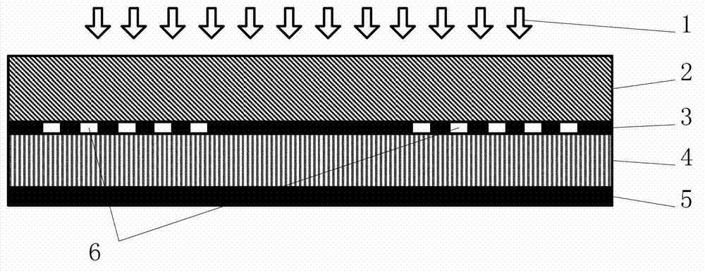
[0059] figure 1 A schematic diagram of nanolithography according to an embodiment of the present invention is shown. Among them, the meaning of each mark is: 1-femtosecond laser; 2-flat light-transmitting substrate; 3-lithography mask, with surface plasmon effect; 4-photoresist, with two-photon absorption effect, (here In the embodiment, it is specifically a negative photoresist, such as SU-82000, SU-82002); 5-substrate; 6-metal structure (the specific structure in this embodiment is a periodic metal grating).

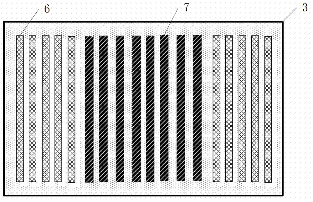
[0060] First, a gold thin film layer of about 100 nm is grown on the flat transparent substrate 2 by magnetron sputtering, vapor deposition, electron beam evaporation and other methods. Then it is prepared by focused ion beam etching, reactive ion etching (RIE) and other methods. figure 2 The metal structure (periodic metal grating) 6 in the photolithography mask 3 with surface plasmon effect is prepared. The metal grating has a period of 480nm and a duty cycle of ...

Embodiment 2

[0062] figure 1 A schematic diagram of nanolithography according to an embodiment of the present invention is shown. First, a gold thin film layer of about 100 nm is grown on the flat transparent substrate 2 by magnetron sputtering, vapor deposition, electron beam evaporation and other methods. Then it is prepared by focused ion beam etching, RIE etching and other methods. figure 2 The metal structure (periodic metal grating) 6 in the photolithography mask 3 with the surface plasmon effect is prepared. figure 2 The period of the metal grating in the middle and the distance between the two groups of gratings are determined according to actual needs. At the same time, a layer of photoresist (positive type) 4 with two-photon absorption effect is spin-coated on the substrate 5 . The substrate 5 coated with the photoresist 4 is placed on a hot plate for baking, and the baking temperature and time depend on the photolithographic conditions. Then the prepared photoresist mask 3...

Embodiment 3

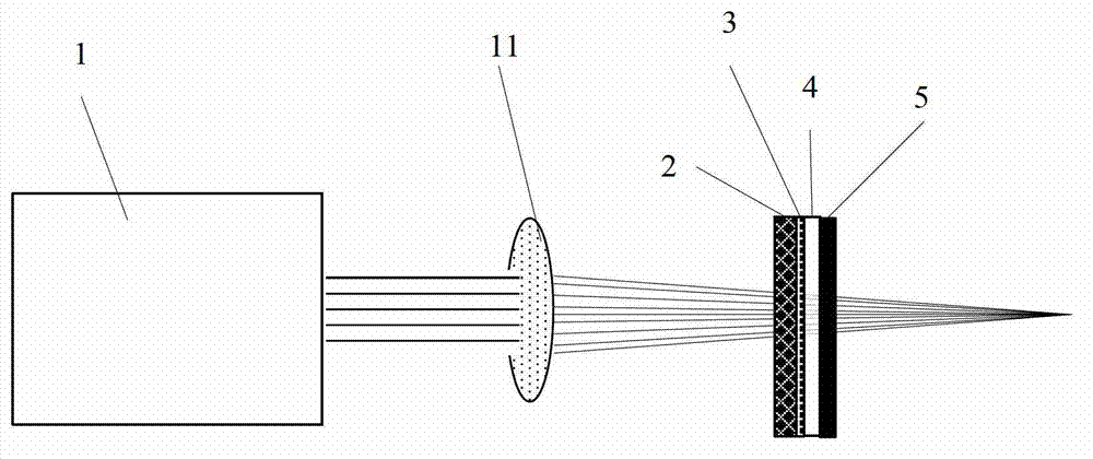
[0064] figure 1 A schematic diagram of nanolithography according to an embodiment of the present invention is shown. The wavelength of the femtosecond laser 1 used in this embodiment can be set according to actual conditions. By changing the wavelength, the dielectric constant of the stencil material is matched with the dielectric constant of the photoresist, so as to further reduce the period of the photolithographic pattern, such as Figure 5 shown. According to the wavelength of the selected light source, the corresponding structural parameters, such as the thickness of the gold film and the period of the metal grating, are designed through theoretical calculations. A gold thin film layer with a certain thickness is grown on the flat transparent substrate 2 by means of magnetron sputtering, evaporation, electron beam evaporation and the like. Then it is prepared by focused ion beam etching, RIE etching and other methods. figure 2 The metal structure (periodic metal gra...


PUM


Abstract

The invention discloses a nanolithography method and a nanolithography device in the technical field of nanolithography. The device comprises a femtosecond laser device, a light transmittance base plate, a photoetching mask plate, photoresist and a substrate. A specific super-diffraction limit graph is formed on the photoetching mask plate through the femtosecond laser device; a plasma excimer excitation structure on the upper surface of the photoetching mask plate is changed, and an exposure wavelength is adjusted by controlling the material of the photoetching mask plate, so that the shape, the distribution and the size of the super-diffraction limit graph can be controlled; moreover, a two-photon absorption phenomenon of the photoresist is introduced; and the line width of an exposure graph of the photoresist is controlled by controlling the power of a femtosecond laser exposure light source.

Description

technical field [0001] The invention relates to the technical field of nano-lithography, in particular to a nano-lithography method and device. Background technique [0002] Nanolithography is a very important step in micro-nano processing technology. However, due to the existence of the optical diffraction limit, nanolithography cannot further reduce the size of the device and improve the processing accuracy. Currently, shrinking the exposure wavelength in lithography is the most effective solution. The exposure wavelength in nanolithography has been further reduced from the initial 365 nm (i-line) to today's 193 nm. At the same time, people are also studying the related technologies of the extreme deep ultraviolet wavelength (EUV, 13nm) to meet the requirements of future device sizes. While reducing the wavelength, people have also come up with many technical means to improve the processing accuracy of current lithography, such as phase shift mask technology, oil immers...

Claims


Application Information

Patent Timeline
IPC IPC(8): G03F7/00G03F7/20G02F1/35
Inventor 刘仿李云翔黄翊东肖龙
Owner TSINGHUA UNIV
Why Eureka
Try Eureka