Nano composite Cr-Al-O (chromium-aluminum-oxygen) solar spectrum selective absorption coating and preparation method thereof
A solar spectrum and selective absorption technology, which is applied in the field of nanocomposite Cr-Al-O solar spectrum selective absorption coating and its preparation, can solve the problem of low cost, less research on the optical properties and microstructure of the coating, and high ion energy. and other problems, to achieve the effect of overcoming poor adhesion, good industrial application prospects and simple equipment structure
- Summary
- Abstract
- Description
- Claims
- Application Information
AI Technical Summary
Problems solved by technology
Method used
Image
Examples
preparation example Construction
[0044] The preparation process of this present embodiment is:
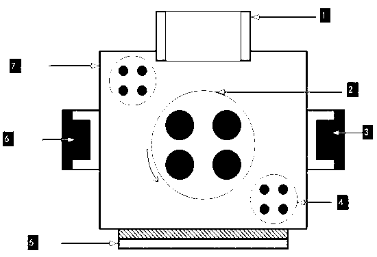
[0045] First, the cleaning of the base material. The base material was ultrasonically cleaned in acetone, alcohol, and deionized water for 15 minutes each, then dried in a desiccator, and then loaded on a workpiece rack whose rotation speed could be adjusted between 3-5 rpm, and the door of the sample preparation chamber was closed.
[0046] Second, the acquisition of a vacuum environment. The first is to use a mechanical pump to pump air under low vacuum conditions; when the vacuum degree reaches below 2pa, turn on the molecular pump to convert the pumping system into a high vacuum system until 8×10 -3 below pa.
[0047] Third, the preparation of the coating. First set the rotating speed of the workpiece holder to 3-5rpm. Then use high-power (1.4-1.6 kilowatts) arc discharge technology to evaporate Cr ions from the Cr target with current, and deposit them on the rotating substrate connected to the negative bi...
Embodiment 1
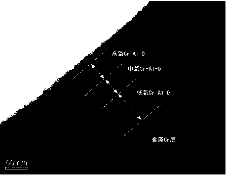
[0050] Embodiment one: at 10 -3 Under the vacuum degree, the control speed is 3rpm, and the high-energy ions evaporated from the Cr target are used to deposit the Cr layer on the cleaned stainless steel substrate. The power of the deposition source is 1.4 kilowatts, the bias voltage on the workpiece is -800V, and the deposition time is 10min. The thickness of the infrared high reflection layer is 500 nanometers; after the deposition is completed, reduce the bias voltage to -100V, feed in oxygen with a flow rate of 15SCCM, and adjust the argon flow rate to make the vacuum degree 0.4Pa, open the CrAl target, and the current is 30A, The corresponding power is 0.6 kilowatts, and the hypoxic absorbing layer is deposited, and the hypoxic absorbing layer is Cr-Al alloy nanocrystal and amorphous phase (Al 2 Cr)-O X The composite material, the deposition time is 2min, where X is 0.67, the thickness is 65 nanometers, and the size of the metal nanocrystal is 4-5 nanometers; the oxygen f...
Embodiment 2
[0051] Embodiment two: at 10 -2 Under the vacuum degree, the control speed is 5rpm, and the high-energy ions evaporated from the Cr target are used to deposit the Cr layer on the cleaned stainless steel substrate. The power of the deposition source is 1.6 kilowatts, the bias voltage on the workpiece is -1000V, and the deposition time is 10min. The thickness of the infrared high reflection layer is 600 nanometers; after the deposition is completed, reduce the bias voltage to -200V, feed in oxygen with a flow rate of 20SCCM, and adjust the argon flow rate to make the vacuum degree 0.5Pa, open the CrAl target, and the current is 40A, The corresponding power is 0.8 kilowatts, and the hypoxic absorbing layer is deposited. The hypoxic absorbing layer is Cr-Al alloy nanocrystal and amorphous phase (Al 2 Cr)-O X The composite material, the deposition time is 2min, where X is 0.7, the thickness is 70 nanometers, and the size of metal nanocrystals is 3-5 nanometers; the oxygen flow rat...
PUM
 Abstract
Description
Claims
Application Information


