Method for preparing tungsten trioxide film based room temperature gas sensor element

A gas sensor, tungsten trioxide technology, applied in the direction of material resistance, etc., can solve the problems of unfavorable gas sensor integration and intelligence, resistance increase, high power consumption, etc.

Inactive Publication Date: 2014-01-15
TIANJIN UNIV
View PDF6 Cites 15 Cited by
  • Summary
  • Abstract
  • Description
  • Claims
  • Application Information

AI Technical Summary

Problems solved by technology

At present, the tungsten trioxide film material studied by researchers at home and abroad and our research group based on the gas-sensing characteristics is an n-type semiconductor. When placed in the air, the surface of the film will absorb oxygen ions, and oxidized gases (such as NO 2 etc.) after contact, the conductivity decreases and the resistance increases, and the change in resistance is proportional to the concentration of the detected gas, but the operating temperature of the n-type tungsten trioxide semiconductor thin film gas sensor is generally above 200 ° C, and the power consumption is large, which is not conducive to the realization Integration and intelligence of gas sensors

Method used


Image

  • Method for preparing tungsten trioxide film based room temperature gas sensor element
  • Method for preparing tungsten trioxide film based room temperature gas sensor element
  • Method for preparing tungsten trioxide film based room temperature gas sensor element

Examples


Embodiment 1

[0028] 1) Silicon wafer cleaning

[0029] Cut a p-type single-sided polished single-crystal silicon wafer with a resistivity of 10-15Ω·cm, a thickness of 400μm, and a crystal orientation into a rectangular silicon substrate with a size of 2.5cm×1cm, and put it into the prepared hydrogen peroxide : Soak in concentrated sulfuric acid = 1:3 cleaning solution for 40 minutes to remove surface organic pollutants; rinse with deionized water and soak in 5% hydrofluoric acid aqueous solution for 30 minutes to remove surface oxide layer; rinse with deionized water Then put it into acetone solvent, absolute ethanol, and deionized water for ultrasonic cleaning for 15 minutes, respectively, to clean off the ions and organic impurities on the surface, and dry it for later use.

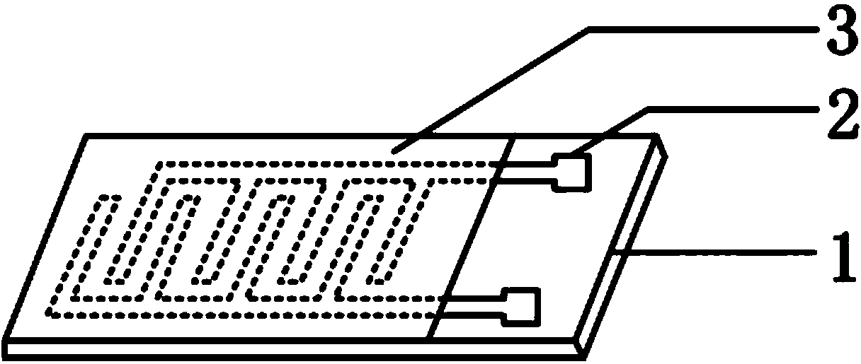
[0030] 2) Sputtering platinum interdigitated electrodes

[0031] The cleaned and dried p-type single crystal silicon substrate samples were placed in the vacuum chamber of the DPS-Ⅲ ultra-high vacuum counter-targe...

Embodiment 2

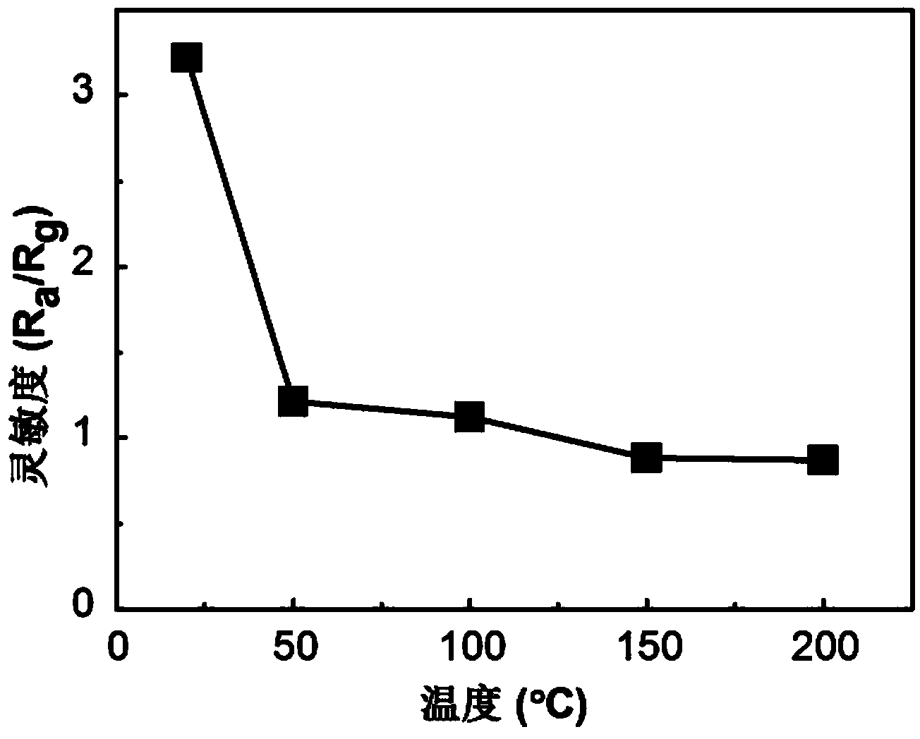
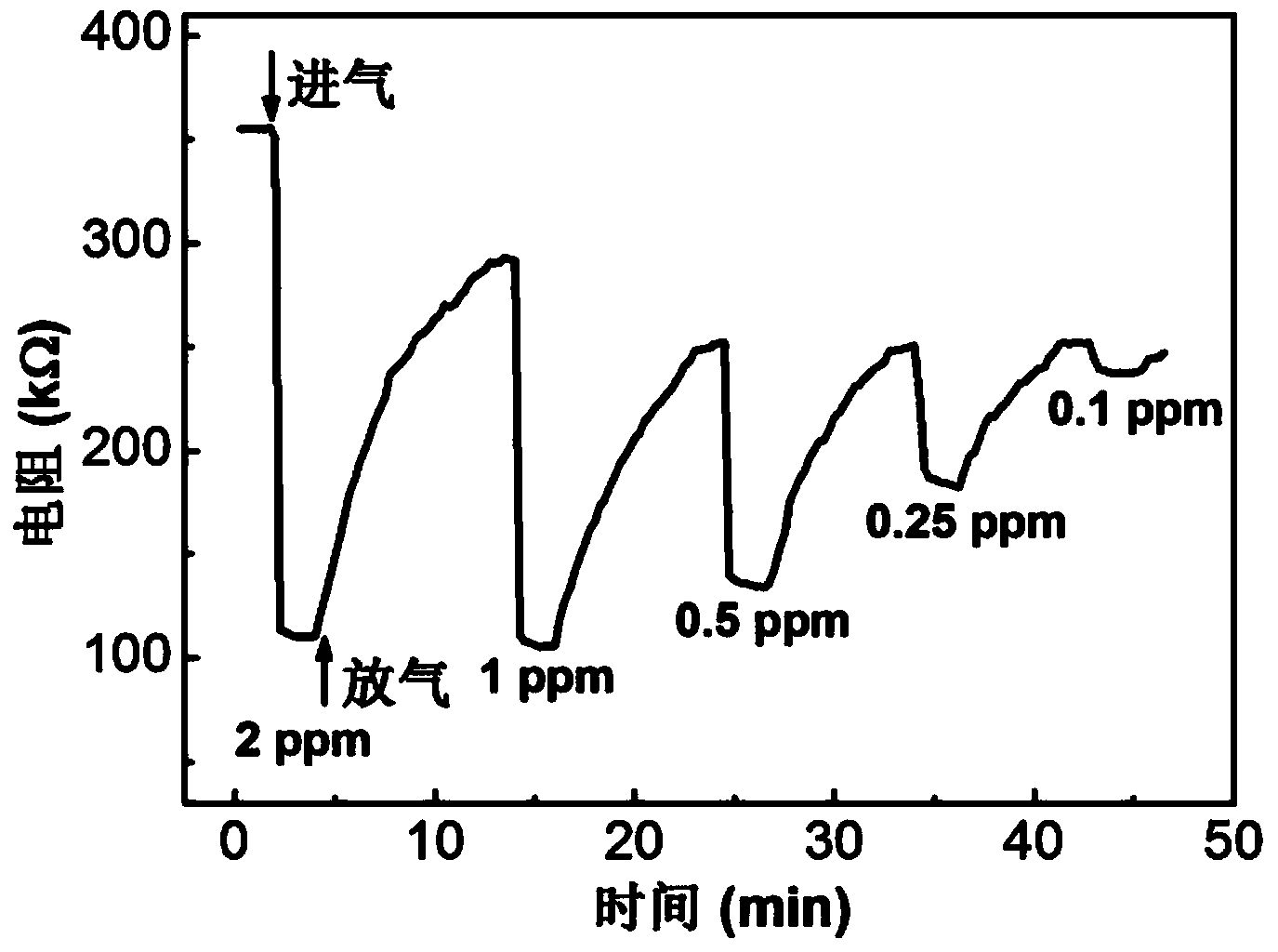
[0038] The difference between this example and Example 1 is that the heat treatment temperature of the sample substrate after spin coating in step 3) is 350°C, and the prepared silicon-based tungsten trioxide thin film gas sensor element is resistant to 2ppm NO at room temperature. 2 The sensitivity is 1.03, showing the gas-sensing characteristics of p-type semiconductors.

Embodiment 3

[0040]The difference between this example and Example 1 is that the heat treatment temperature of the sample substrate after spin coating in step 3) is 500°C, and the prepared silicon-based tungsten trioxide thin film gas sensor element is resistant to 2ppm NO at room temperature. 2 Shown as the gas-sensing characteristic of p-type semiconductor, the sensitivity is 1.84.


PUM

PropertyMeasurementUnit
thicknessaaaaaaaaaa
electrical resistivityaaaaaaaaaa
quality scoreaaaaaaaaaa

Abstract

The invention provides a method for preparing a tungsten trioxide film based room temperature gas sensor element, wherein a p-type monocrystalline silicon is taken as a substrate, platinum is taken as a target, and a platinum interdigital electrode is formed on a glazed surface of the silicon substrate through sputtering; then a sol-gel spin-coating method is used to deposit the tungsten trioxide film on the glazed surface of the silicon substrate with sputtered platinum interdigital electrode, wherein the precursor is a sol prepared from tungsten hexachloride and absolute ethyl alcohol at the mass ratio of (0.8-1):10; and then the product is put in a muffle furnace to be subjected to heat treatment. The invention provides the method for preparing the low-power-consumption and easy-in- silicon-substrate-integration tungsten trioxide film based gas sensor element, and the method can detect the low-concentration (0.1ppm) nitrogen dioxide gas at the room temperature and has the advantages of high sensitivity, rapid response / recovery, good selectivity and good repeatability.

Description

technical field [0001] The invention relates to a gas sensor, in particular to a preparation method of a silicon-based tungsten trioxide film-based nitrogen dioxide gas sensor element working at room temperature. Background technique [0002] The increasing development of modern industry has brought inevitable damage to the ecological environment while improving people's living standards. Nitrogen dioxide emitted from the decomposition of organic matter, the combustion of fossil fuels, and the production process of the chemical industry is a common air pollutant and one of the main substances that form acid rain and photochemical smog, which is extremely harmful to the environment. Therefore, the research on nitrogen dioxide gas sensor elements has important significance and development prospects. [0003] Tungsten trioxide gas-sensing materials have attracted extensive attention from researchers due to their high sensitivity to gases such as nitrogen dioxide and ammonia, s...

Claims


Application Information

Patent Timeline
Patent Type & Authority Applications(China)
IPC IPC(8): G01N27/12
Inventor 胡明闫文君曾鹏马双云李明达
Owner TIANJIN UNIV
Why Eureka
Try Eureka