Manufacturing method of T-shaped gate of GaN-based FET (Field Effect Transistor)

A gallium nitride base field and manufacturing method technology, applied in the field of structural design of high electron mobility field effect transistors, can solve the problem of affecting high-frequency power characteristics of devices, increasing gate-source capacitance and gate-drain capacitance, affecting device frequency performance, etc. problem, to achieve the effect of suppressing the current collapse effect, improving the gate control ability, and improving the power characteristics

Inactive Publication Date: 2014-04-02
INST OF MICROELECTRONICS CHINESE ACAD OF SCI
View PDF3 Cites 7 Cited by
  • Summary
  • Abstract
  • Description
  • Claims
  • Application Information

AI Technical Summary

Problems solved by technology

[0005] The GaN microwave power die with this structure has achieved good power output characteristics in the Ku-band and below the Ku-band. However, due to the parasitic capacitance between the gate and the dielectric, the gate-source capacitance (C gs ) and gate-to-drain capacitance (C gd ) increases, which affects the frequency performance of the device, making it difficult for the device to work in the Ka band and above
[0006] In the Ka-band and above frequency bands, in order to reduce the gate-source and gate-drain parasitic capacitance, the gate structure adopts a T-shaped gate structure. While reducing the gate length, the gate cap is not in contact with the epitaxial layer or the dielectric layer. Due to the air dielectric constant Low, can greatly improve the frequency characteristics of the device, but the traditional T-shaped gate structure will cause current collapse under high field due to the lack of passivation or incomplete passivation on the surface, which will affect the high-frequency power characteristics of the device

Method used


Image

  • Manufacturing method of T-shaped gate of GaN-based FET (Field Effect Transistor)
  • Manufacturing method of T-shaped gate of GaN-based FET (Field Effect Transistor)
  • Manufacturing method of T-shaped gate of GaN-based FET (Field Effect Transistor)

Examples


Embodiment Construction

[0029] In order to make the objectives, technical solutions and advantages of the present invention clearer, the present invention will be further described in detail below with reference to specific embodiments and accompanying drawings.

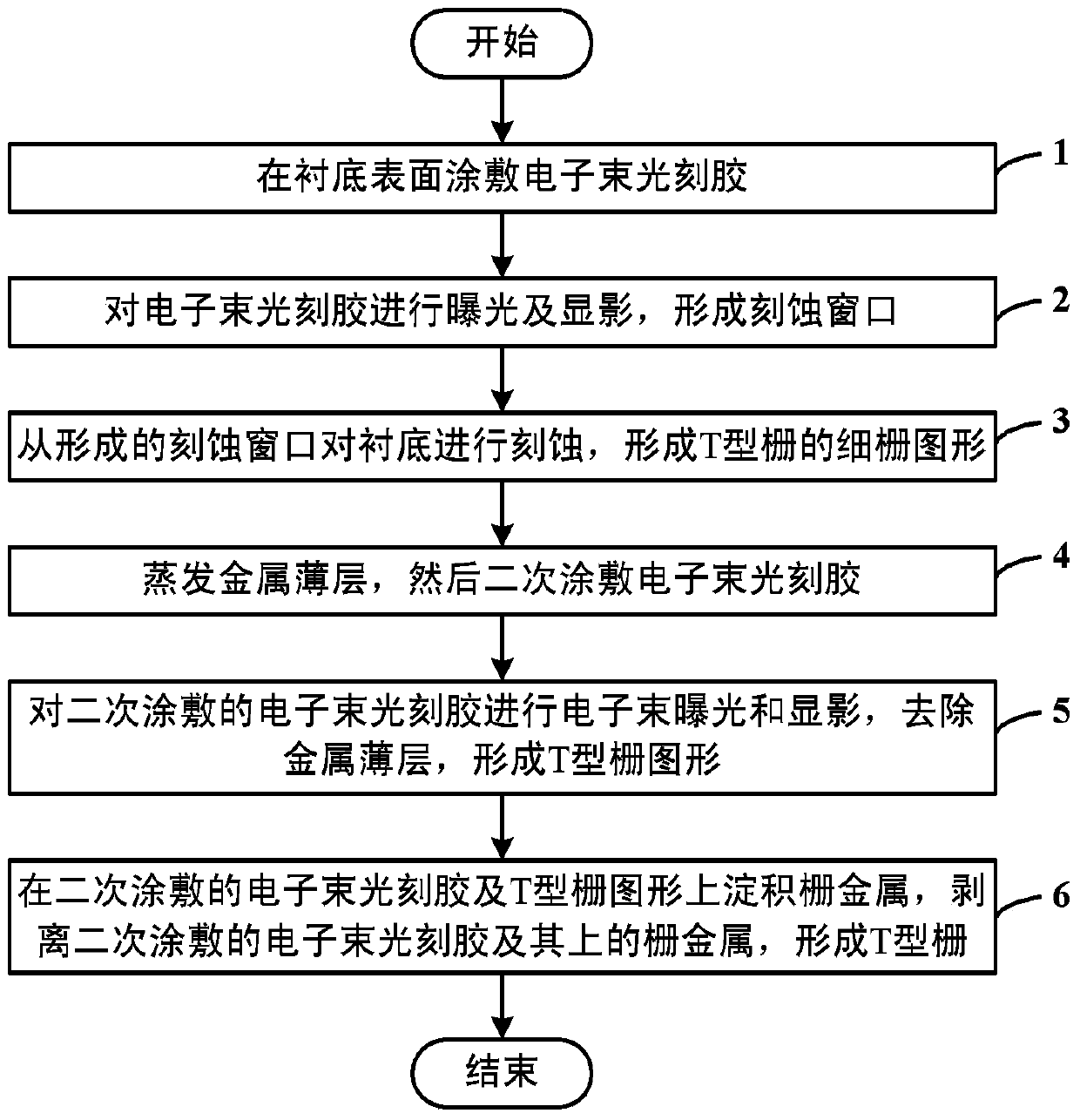
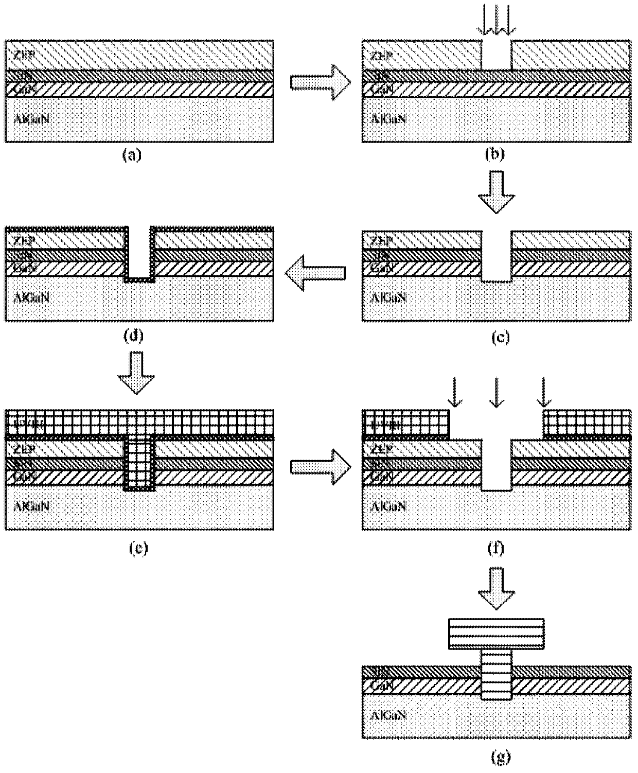
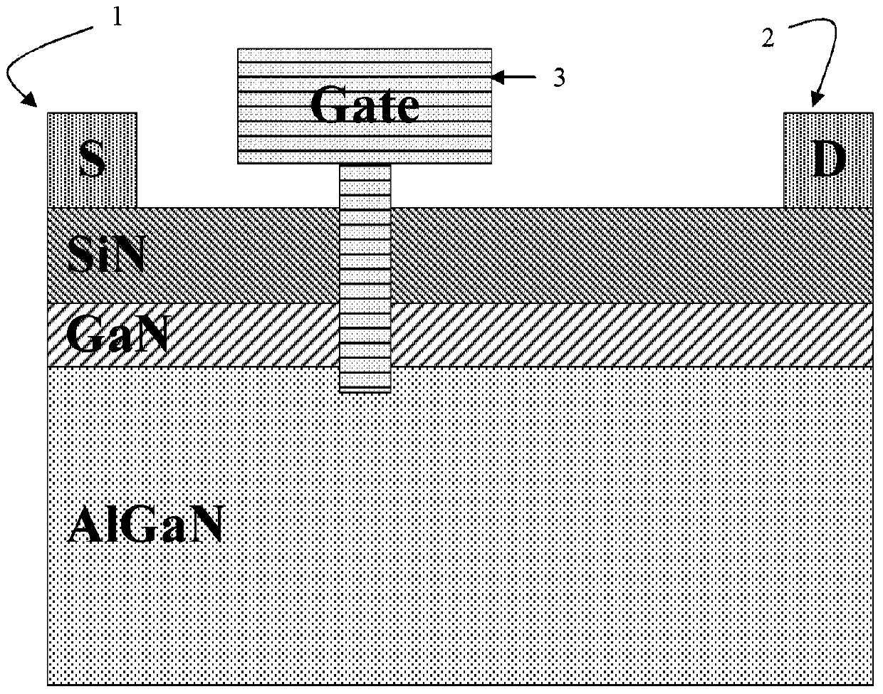
[0030] The invention provides a method for manufacturing a T-type gate of a gallium nitride-based field effect transistor. ZEP520 electron beam photoresist is used for exposure and development to form a fine gate part of the T-type gate. After ICP etching the gate groove, the glue is not removed. , Evaporating metal Al as an isolation layer, uniform electron beam glue UVIII, secondary electron beam lithography, forming a T-type grid, and finally evaporate and peel off to obtain a T-type grid pattern.

[0031] like figure 1 shown, figure 1 It is a flow chart of a method for manufacturing a T-type gate of a GaN-based field effect transistor provided by the present invention, and the method includes the following steps:

[0032] Step 1: appl...


PUM


Abstract

The invention discloses a manufacturing method of a T-shaped gate of a GaN-based FET (Field Effect Transistor). The manufacturing method comprises the steps of coating an electron beam photoresist on the surface of a substrate; carrying out exposure and development on the electron beam photoresist, and forming an etching window; etching the substrate from the formed etching window, and forming a fine gate graph of the T-shaped gate; evaporating a metal thin layer, and then secondly coating the electron beam photoresist; carrying out electron beam exposure and development on the electron beam photoresist which is secondly coated, removing the metal thin layer, and forming a T-shaped gate graph; evaporating deposited gate metal on the electron beam photoresist which is secondly coated and the T-shaped gate graph, stripping the electron beam photoresist which is secondly coated and the gate metal on the electron beam photoresist which is secondly coated, and forming the T-shaped gate. By utilizing the manufacturing method disclosed by the invention, the current collapse is effectively restrained, the stray capacitances of a gate source and a gate drain are reduced, the gate resistance of a device is reduced, the cut-off frequency (ft) and the maximum oscillation frequency (fmax) of the device are increased, and thus the device can work in an MMW (Millimeter Wave) frequency band.

Description

technical field [0001] The invention relates to the technical field of structural design of high electron mobility field effect transistors (HEMTs), in particular to a method for fabricating T-type gates of gallium nitride based field effect transistors suitable for millimeter waves. Background technique [0002] Millimeter-band power amplifiers have great application prospects in military, commercial and consumer fields. High-frequency broadband wireless communication technology, precision guided weapons, long-range radar and space communication technology, the working frequency band has gradually developed from C and X bands to higher frequency bands such as Ku and Ka. [0003] As a third-generation semiconductor material, GaN material has a wide band gap, high breakdown electric field, and high output power. Because it can work under high voltage and has low on-resistance, GaN devices also show higher gain. At the same time, the GaN device has high electron mobility and ...

Claims


Application Information

Patent Timeline
Patent Type & Authority Applications(China)
IPC IPC(8): H01L21/28
CPCH01L29/4236H01L29/401
Inventor 刘果果魏珂孔欣刘新宇
Owner INST OF MICROELECTRONICS CHINESE ACAD OF SCI
Why Eureka
Try Eureka