Improved copper electroplating method of crystal silicon solar battery

A technology of solar cells and copper electroplating, applied in circuits, electrical components, climate sustainability, etc., can solve the problems of reducing the lifetime of minority carriers, prone to amorphous impurities, and reducing electrical conductivity, etc., to improve the manufacturing process Level, the effect of ensuring battery performance and reliability

Active Publication Date: 2014-04-16
GUODIAN NEW ENERGY TECH INST +1
View PDF23 Cites 16 Cited by
  • Summary
  • Abstract
  • Description
  • Claims
  • Application Information

AI Technical Summary

Problems solved by technology

However, after using plate PECVD (Plasma Enhanced Chemical Vapor Deposition) to plate silicon nitride on traditional crystalline silicon cells, it is easy to cause surface patterns when performing Cu electrode plating process; The silicon nitride plating layer is denser, but it is easy to make the silicon nitride layer contain more pin holes in the process of industrial mass production, and Cu is easily adsorbed on the silicon nitride during subsequent Cu electrode plating. layer holes and penetrate into the silicon nitride layer and Si-based interface, affecting battery life and power generation efficiency
Cu is a deep-level impurity, and it

Method used


Image

  • Improved copper electroplating method of crystal silicon solar battery
  • Improved copper electroplating method of crystal silicon solar battery
  • Improved copper electroplating method of crystal silicon solar battery

Examples


specific Embodiment approach

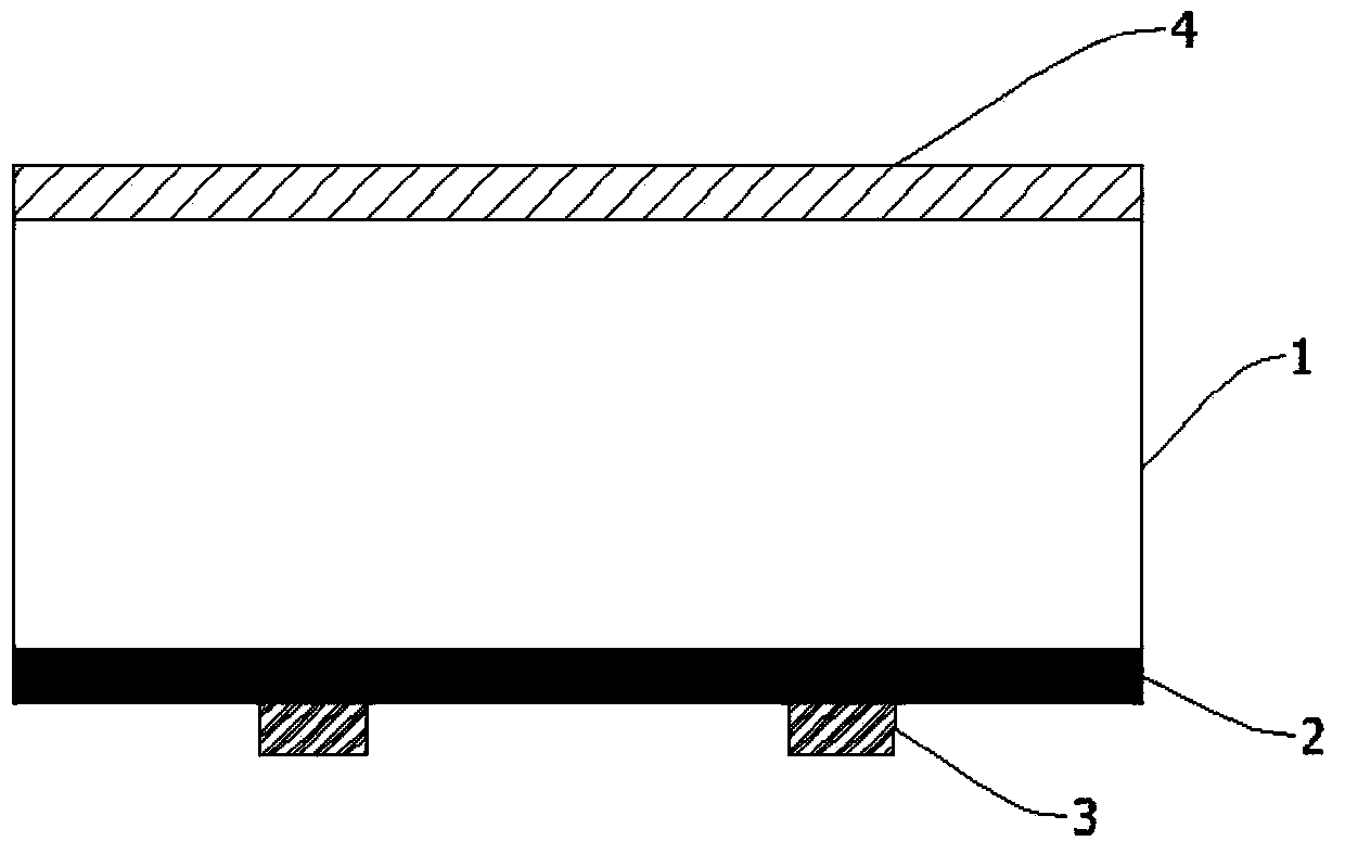
[0035] Such as figure 1 As shown, the main body of the crystalline silicon sample to be processed is a Si base, a silicon nitride layer is deposited on the front side, and a sample with an Al back field structure on the back side.

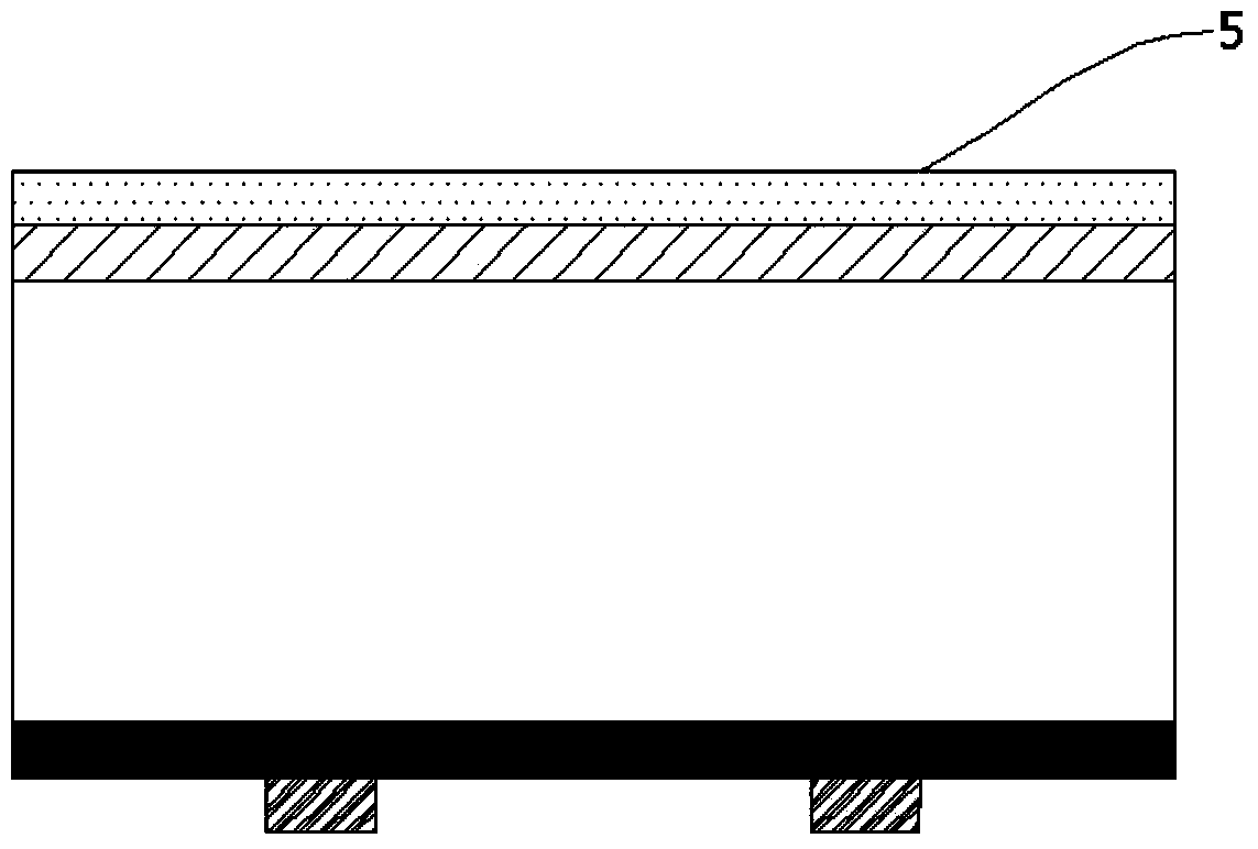
[0036] 1. A mask with openings is covered on the surface of the silicon nitride layer as a protective film, and the positions of the openings correspond to the positions of gate lines to be etched. Methods as below:

[0037] (1) if figure 2 As shown, the surface of the silicon nitride layer of the sample is first covered with a whole layer of photosensitive protective film material, and then the sample is placed in an exposure machine for exposure, and the protective film material at the position of the gate line is removed by development to form the window with a window. Protective film; the protective film used in this scheme is dry film or other photosensitive materials, and the protective film is covered by lamination method, coating method...

Embodiment 1

[0065] Embodiment 1: This embodiment is an improved copper electroplating method for crystalline silicon cells, and the following steps are performed:

[0066] (1) Lamination method to cover the protective film. The protective film uses acid-resistant negative adhesive dry film, which is composed of protective film polyethylene, photoresist film and carrier polyester film;

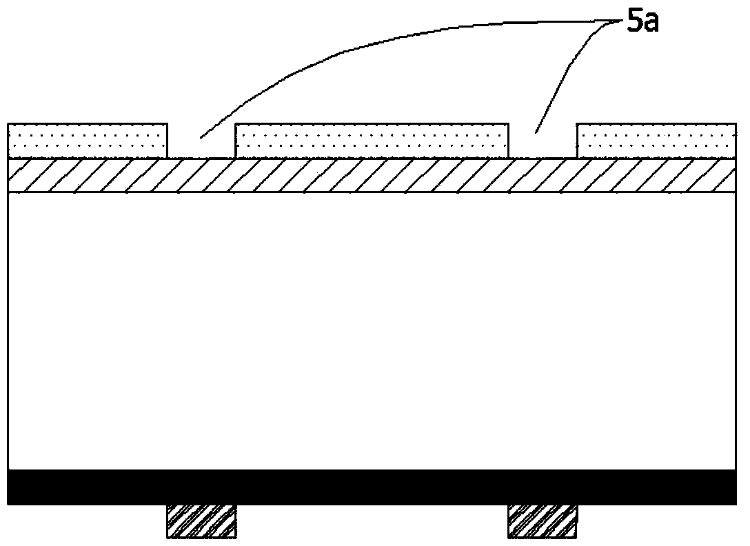
[0067] (2) Exposure and development. The developer is 0.3-4% NaOH solution; the state of the sample after this step is as follows image 3 shown;

[0068] (3) Etching. The etching solution is 10%-35% hydrofluoric acid, and the time is 2-60min; the state of the sample after completing this step is as follows Figure 4 shown;

[0069] (4) Plating barrier layer. The material is Ni, the electroplating method is used, photocatalysis is added, and the sample is placed horizontally; the electroplating anode is a nickel strip, the electroplating temperature is 35-65°C, and the electroplating time is 0-500sec...

Embodiment 2

[0073] Embodiment 2: This embodiment is an improved copper electroplating method for crystalline silicon cells, and the steps different from Embodiment 1 are:

[0074] (1) Plating barrier layer. The material is Ni, using electroless plating, adding photocatalysis, and the sample is placed horizontally; the electroless plating solution is sodium hypophosphite solution; the temperature is 30-95°C, and the time is 0.5-30min;

[0075] (2) Increase the anti-oxidation layer. The material is Sn, the electroplating method is adopted, and the sample is placed horizontally; the electroplating solution is methanesulfonate;

[0076] All the other steps are the same as in Example 1.


PUM

PropertyMeasurementUnit
Thicknessaaaaaaaaaa
Thicknessaaaaaaaaaa

Abstract

The invention relates to an improved copper electroplating method of a crystal silicon solar battery. The silicon nitride layer on the surface of the conventional battery has many pin holes, and in the process of preparing copper (Cu) electrodes by an electroplating process, the Cu electrodes are easy to be adsorbed to the pin holes of the silicon nitride layer to lead to blur in appearance of the solar battery. Meanwhile, the copper electrodes are easy to seep into the silicon nitride layer and a silicon-based interface through the pin holes, and Cu as a deep energy level impurity with very fast diffusion rate entering into a pn junction affects the service life and generating efficiency of the battery, so that the reliability of the battery is reduced. A protective film covers the surface of the silicon nitride layer before Cu electroplating to prevent Cu from being adsorbed and seeped in the electroplating process, so that the reliability of the battery is guaranteed while the blur in appearance of the solar battery is avoided. The protective film can be removed after Cu electrode electroplating. According to the technological requirements of the crystal silicon batteries, the protective film can be still remained if parameters of the battery such as optical and electrical properties and reliability are not affected.

Description

technical field [0001] The invention relates to a manufacturing process of a crystalline silicon solar cell, in particular to an improved copper electroplating method for a crystalline silicon solar cell. Background technique [0002] With the increasingly tense global resources, solar energy has unique advantages such as no pollution, no mechanical rotating parts, easy maintenance, unattended operation, short construction period, random scale, easy combination with buildings, and large market space. The advantages are widely valued by countries all over the world, and many large companies in the world have invested in the research and development and production of solar cells. With the development of technology in the past ten years, although the application cost of silicon solar cells has dropped significantly, in order to meet the needs of wide application in real life, it is necessary to further reduce the manufacturing cost and at the same time further increase the conv...

Claims


Application Information

Patent Timeline
IPC IPC(8): C25D7/12C25D5/02C25D3/38H01L31/0216H01L31/18
CPCY02P70/50
Inventor 郭桦陈锐李玮阚东武段光亮蔡晓晨
Owner GUODIAN NEW ENERGY TECH INST
Why Eureka
Try Eureka