A Coating Equipment Combined with Pulse Laser Deposition and Molecular Beam Epitaxy and Its Application
A technology of pulsed laser deposition and molecular beam epitaxy, which is applied in photodetectors, laser diodes, light emitting diodes, thin film epitaxy and thin film devices, and solar cells, can solve the problems of limited promotion and application range, and reduce production costs. The effect of suppressing the interface reaction and saving the cost of equipment procurement
- Summary
- Abstract
- Description
- Claims
- Application Information
AI Technical Summary
Problems solved by technology
Method used
Image
Examples
Embodiment 1
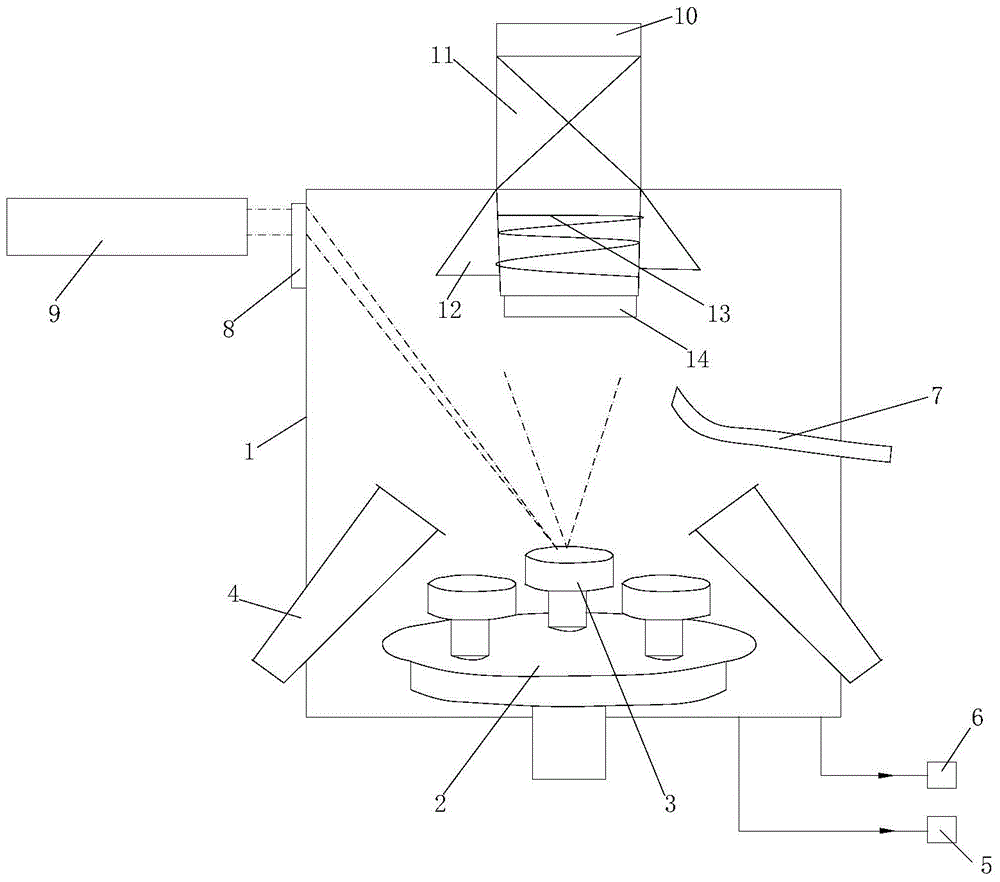
[0051] Please refer to figure 1 , a pulsed laser deposition combined with molecular beam epitaxy coating equipment, which includes a growth chamber cavity 1;
[0052] A base 2 is provided at the center below the growth chamber cavity 1, and 1-6 evenly arranged turntables 3 for placing targets are arranged on the base 2, and the base 2 and the turntable 3 are respectively composed of The driving mechanism drives the rotation, so that the target can not only revolve with the base 2 but also rotate with the turntable 3;
[0053] Several evenly distributed MBE evaporation sources 4 are also provided on the lower side wall of the growth chamber cavity 1;
[0054] Valves connected to the mechanical pump 5 and the molecular pump 6 are also provided on the lower side wall or the bottom wall of the growth chamber cavity 1, so that the mechanical pump 5 and the molecular pump 6 vacuumize the growth chamber;
[0055] An auxiliary gas pipeline 7 and RF accessories are provided at the mi...
Embodiment 2
[0061] The method for preparing non-polar GaN-based LED epitaxial wafers by using pulsed laser deposition and molecular beam epitaxy combined with coating equipment is carried out according to the following steps:
[0062] 1) Selection of substrate and its crystal orientation: use LiGaO 2 The substrate, with the (100) plane offset from the (110) direction by 0.2° as the epitaxial plane, the crystal epitaxial orientation relationship is: the (1-100) plane of GaN is parallel to LiGaO 2 (100) faces.
[0063] 2) polishing, cleaning and annealing the surface of the substrate;
[0064] The polishing process is specifically: firstly LiGaO 2 The surface of the substrate is polished with diamond slurry, and the surface of the substrate is observed with an optical microscope until there are no scratches, and then polished by chemical mechanical polishing;
[0065] The cleaning treatment is specifically: the LiGaO 2 The substrate was ultrasonically cleaned in deionized water for 3 mi...
Embodiment 3
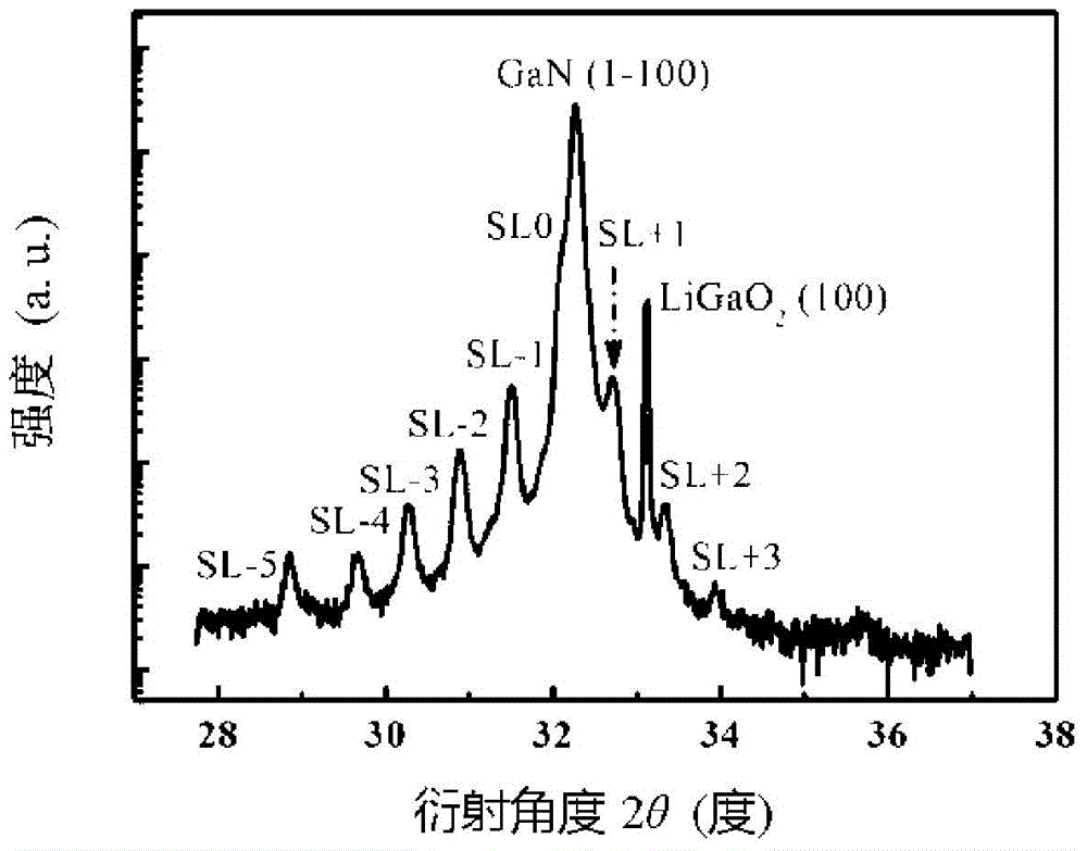
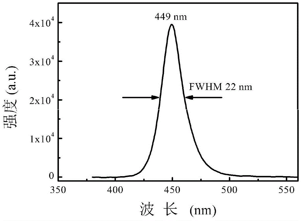
[0078] The GaN thin film grown on the lithium gallate substrate was prepared by using the pulsed laser deposition and molecular beam epitaxy coating equipment described in Example 1, and the GaN thin film was used to prepare LED: after growing on the lithium gallate substrate Si-doped n-type silicon-doped GaN and In are epitaxially grown sequentially on the GaN film on x Ga1-xN multi-quantum well layer, Mg-doped p-type magnesium-doped GaN layer, and finally electron beam evaporation to form ohmic contact. The GaN-based LED device prepared on the lithium gallate substrate has a thickness of n-type GaN of about 4.5 μm and a carrier concentration of 1.7×10 19 cm -3 ;In x Ga 1-x The thickness of the N / GaN multi-quantum well layer is about 150nm, and the number of periods is 10, where In x Ga 1-x The N well layer is 3nm, the GaN barrier layer is 12nm, the thickness of the p-type magnesium-doped GaN layer is about 300nm, and the carrier concentration is 4.9×10 17 cm -3 . Und...
PUM
| Property | Measurement | Unit |
|---|---|---|
| thickness | aaaaa | aaaaa |
| thickness | aaaaa | aaaaa |
| thickness | aaaaa | aaaaa |
Abstract
Description
Claims
Application Information


