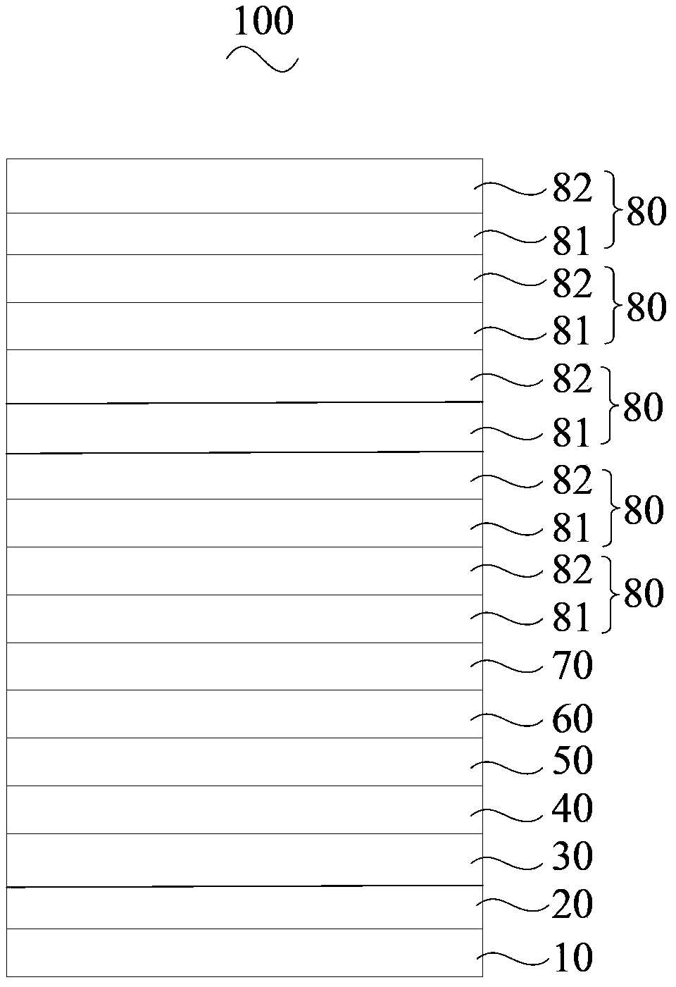
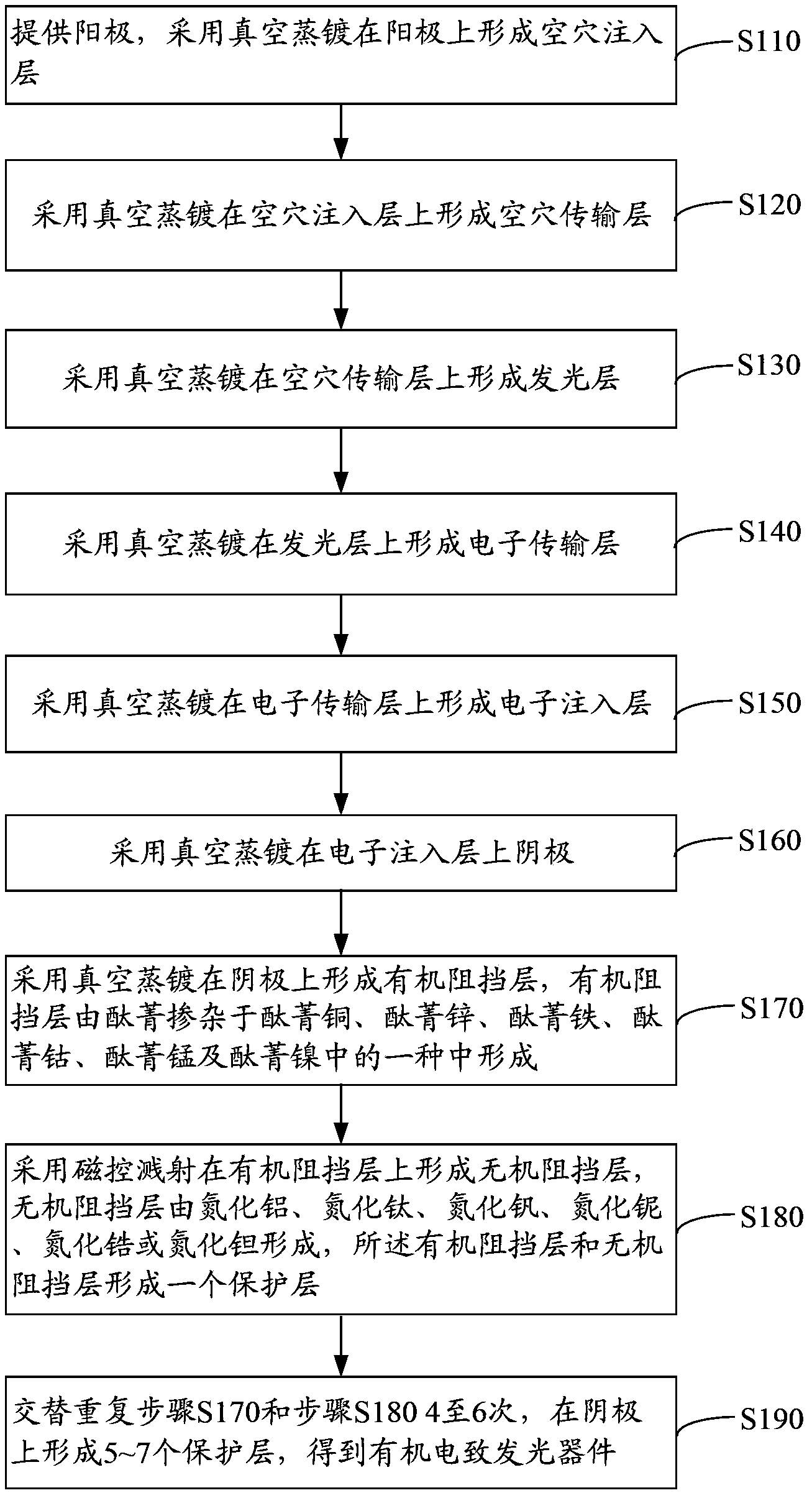
Organic electroluminescent device and packaging method thereof
A technology of electroluminescent devices and encapsulation methods, which is applied to organic semiconductor devices, organic semiconductor device materials, electric solid devices, etc., and can solve problems such as low service life, easy to be corroded, and reduced luminous quantum efficiency, and achieve service life high effect
- Summary
- Abstract
- Description
- Claims
- Application Information
AI Technical Summary
Problems solved by technology
Method used
Image
Examples
Embodiment 1
[0096] The structure is ITO / MoO 3 :NPB / TCTA / Ir(ppy) 3 :TPBI / Bphen / CsN 3 :Bphen / Al / (H 2 Pc:CuPc / AIN) 7 Encapsulation of organic electroluminescent devices
[0097] (1) Provide an anode, the anode is indium tin oxide glass, expressed as ITO. First, put the anode into acetone, ethanol, deionized water and ethanol for ultrasonic cleaning, each ultrasonic cleaning for 5 minutes, then blow dry with nitrogen, and then dry in an oven to obtain a clean and dry anode. Further use UV-ozone (UV-ozone) to treat the cleaned and dried anode for surface activity treatment for 30 minutes to increase the oxygen content on the surface of the anode and improve the work function of the anode;
[0098] (2) The hole injection layer formed on the surface of the anode by vacuum evaporation, the vacuum degree of vacuum evaporation is 1×10 -5 Pa, the evaporation rate is The hole injection layer is made of molybdenum trioxide (MoO 3 ) doped in N,N'-diphenyl-N,N'-di(1-naphthyl)-1,1'-biphenyl-4,4'...
Embodiment 2
[0108] The structure is ITO / MoO 3 :NPB / TCTA / Ir(ppy) 3 :TPBI / Bphen / CsN 3 :Bphen / Al / (H 2 Pc:ZnPc / TiN) 7 Encapsulation of organic electroluminescent devices
[0109] In steps (1) to (7), the rest is the same as that in Example 1, except that the time for surface activation treatment on the anode is 50 minutes.
[0110] (8) Vacuum evaporation is used to form an organic barrier layer on the cathode, and the vacuum degree of vacuum evaporation is 5×10 -5 Pa, the evaporation rate is The organic barrier layer is composed of phthalocyanine (H 2 Pc) doped in one of the zinc phthalocyanines (ZnPc), denoted as H 2 Pc: ZnPc, wherein, phthalocyanine (H 2 The molar ratio of Pc) to zinc phthalocyanine (ZnPc) is 3:100; the thickness of the organic barrier layer is 150 nm;
[0111] (9) Magnetron sputtering is used to form an inorganic barrier layer on the organic barrier layer, and the vacuum degree of the background is 1×10 -5 Pa; The flow rate of the argon gas that feeds in the mag...
Embodiment 3
[0114] The structure is ITO / MoO 3 :NPB / TCTA / Ir(ppy) 3 :TPBI / Bphen / CsN 3 :Bphen / Al / (H 2 Pc:FePc / VN) 7 Encapsulation of organic electroluminescent devices
[0115] In steps (1) to (7), the rest is the same as that in Example 1, except that the time for surface activation treatment on the anode is 40 minutes.
[0116] (8) Vacuum evaporation is used to form an organic barrier layer on the cathode, and the vacuum degree of vacuum evaporation is 5×10 -5 Pa, the evaporation rate is The organic barrier layer is composed of phthalocyanine (H 2 Pc) doped in one of iron phthalocyanine (FePc), denoted as H 2 Pc: FePc, wherein, phthalocyanine (H 2 The molar ratio of Pc) to iron phthalocyanine (FePc) is 1:100; the thickness of the organic barrier layer is 100 nm;
[0117] (9) Magnetron sputtering is used to form an inorganic barrier layer on the organic barrier layer, and the vacuum degree of the background is 1×10 -5 Pa; The flow rate of the argon gas that feeds in the magnetron...
PUM
| Property | Measurement | Unit |
|---|---|---|
| Thickness | aaaaa | aaaaa |
| Thickness | aaaaa | aaaaa |
Abstract
Description
Claims
Application Information
 - R&D
- Intellectual Property
- Life Sciences
- Materials
- Tech Scout
- Unparalleled Data Quality
- Higher Quality Content
- 60% Fewer Hallucinations
Browse by: Latest US Patents, China's latest patents, Technical Efficacy Thesaurus, Application Domain, Technology Topic, Popular Technical Reports.
© 2025 PatSnap. All rights reserved.Legal|Privacy policy|Modern Slavery Act Transparency Statement|Sitemap|About US| Contact US: help@patsnap.com


