Preparation method of organic-inorganic perovskite solar battery
A technology of solar cells and inorganic calcium, which can be used in circuits, photovoltaic power generation, electrical components, etc., and can solve problems such as high cost, uncontrollable surface morphology, and limited development.
- Summary
- Abstract
- Description
- Claims
- Application Information
AI Technical Summary
Problems solved by technology
Method used
Image
Examples
Embodiment 1
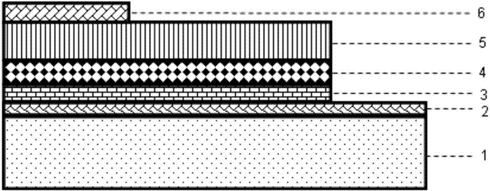
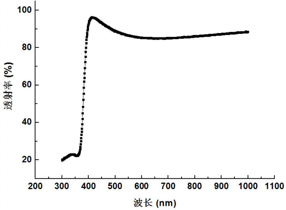
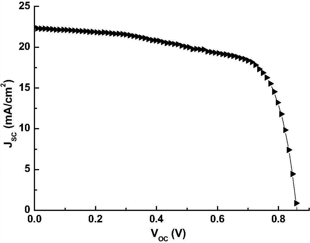
[0050] Example 1 Preparation of planar structure organic-inorganic perovskite solar cells
[0051] (1) Processing and cleaning of AZO glass substrates: Cut the glass substrates into appropriate sizes, then place the glass substrates in acetone, alcohol, and deionized water for 15 minutes, then dry them with pure nitrogen, and immediately use ultraviolet ozone to clean the surface Treat for 12 minutes; (2) Etching of AZO transparent conductive oxide: use pulse laser to etch the pretreated AZO transparent conductive film, then place it in acetone, alcohol, and deionized water for ultrasonic cleaning for 15 minutes, and use Pure nitrogen is blown dry; (3) the preparation of n-type ZnO semiconductor layer: utilize magnetron sputtering method to prepare ZnO thin film on the AZO conductive layer that etches, and magnetron sputtering preparation process is: adopt purity to be 99.99% Zinc oxide ceramic target, the vacuum degree of the vacuum chamber is 1×10 -4 Pa, argon flow rate is ...
Embodiment 2
[0052] Example 2 Preparation of planar structure organic-inorganic perovskite solar cells
[0053] (1) Processing and cleaning of FTO glass substrates: Cut the glass substrates into appropriate sizes, then place the glass substrates in acetone, alcohol, and deionized water for 15 minutes for ultrasonic cleaning, then dry them with pure nitrogen, and immediately use ultraviolet ozone to surface Treat for 12 minutes; (2) Etching of transparent conductive oxide: use 0.1M dilute hydrochloric acid and zinc powder to etch the pretreated FTO transparent conductive film, and then place it in acetone, alcohol, deionized water and ultrasonic Cleaning for 15 minutes, and drying with pure nitrogen; (3) Depositing strontium titanate as an n-type metal oxide semiconductor layer on the pretreated and etched FTO by using a pulsed laser. The preparation process of its strontium titanate n-type layer is as follows: using 99.99% strontium titanate ceramic target, using pulsed laser deposition te...
PUM
| Property | Measurement | Unit |
|---|---|---|
| thickness | aaaaa | aaaaa |
| thickness | aaaaa | aaaaa |
| transmittivity | aaaaa | aaaaa |
Abstract
Description
Claims
Application Information


