Technology for preparing multilayer film thermoelectric materials through physical vapor deposition method

A technology of physical vapor deposition and thermoelectric materials, which is applied in the field of preparation of functional device materials, can solve the problems that cannot meet the needs of the development and application of thermoelectric materials, the combination of samples and substrates is not good, and the purity of the multilayer film structure is affected. The composition and thickness are controllable, the boundary of the film layer is obvious, and the effect of overcoming the poor thermoelectric performance

Inactive Publication Date: 2015-04-22
SHANGHAI UNIV
View PDF4 Cites 8 Cited by
  • Summary
  • Abstract
  • Description
  • Claims
  • Application Information

AI Technical Summary

Problems solved by technology

[0005] Chemical methods mainly include double-tank method and single-tank method, which have the following disadvantages when preparing multilayer films: cross-contamination of solutions in different layers is likely to affect the purity of the multilayer film structure; many factors in the reaction process result in inconsistent experimental results. Good, such as environmental humidity, drug purity and gas impurities, etc.; the combi

Method used


Image

  • Technology for preparing multilayer film thermoelectric materials through physical vapor deposition method
  • Technology for preparing multilayer film thermoelectric materials through physical vapor deposition method
  • Technology for preparing multilayer film thermoelectric materials through physical vapor deposition method

Examples


Embodiment 1

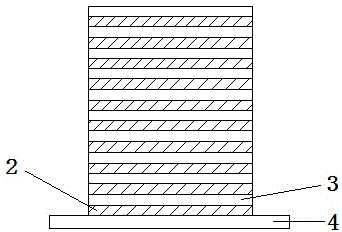
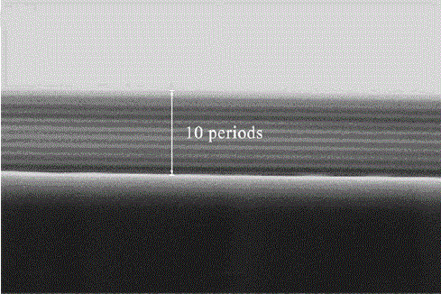
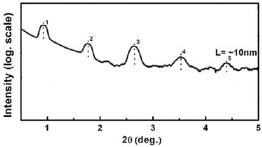
[0024] In this example, see Figure 1 ~ Figure 3 , a process for preparing a multilayer thermoelectric material by physical vapor deposition method, comprising the following steps:

[0025] a. Selection and treatment of the substrate: select the substrate type as Si, and its resistivity is 1000 Ω·cm. First, use BOE solution (hydrogen fluoride: ammonium fluoride = 1:5) to soak the Si substrate for 5 minutes for hydrofluoric acid treatment, then use acetone and ethanol solutions for ultrasonic cleaning for 10 minutes, then use acetone, absolute ethanol, The silicon wafers were cleaned successively with deionized water, then dried with high-purity nitrogen, and finally placed in a drying oven at 80 °C for 15 minutes before being used;

[0026] b. Selection of target material: select silicon and silicon germanium materials with a mass percentage purity of 99.99% as the target material, wherein the silicon germanium material includes 25wt% silicon and 75wt% germanium;

[0027] c....

Embodiment 2

[0033] This embodiment is basically the same as Embodiment 1, especially in that:

[0034] In this example, see Figure 4 , a process for preparing a multilayer thermoelectric material by physical vapor deposition method, comprising the following steps:

[0035] a. selection of substrate and its processing: this step is the same as in Example 1;

[0036] b. Selection of target materials: silicon and gold with a mass percentage purity of 99.99% are selected as target materials;

[0037] c. Fabricate multilayer thermoelectric materials on the substrate: the background vacuum is 5×10 -7 Torr, the substrate is not heated, and the substrate speed is kept at 20rpm. Use RF mode to sputter silicon, and DC mode to sputter gold. The sputtering power of silicon is 100 W, and its deposition rate is about 0.2 ? / s. The radiation power is 25W, the deposition rate is about 0.6 ? / s, and the film thicknesses of silicon and gold are controlled to be 12 nm and 16 nm respectively. The gold la...

Embodiment 3

[0041] This embodiment is basically the same as the previous embodiment, and the special features are:

[0042] In this example, see Figure 5 , a process for preparing a multilayer thermoelectric material by physical vapor deposition method, comprising the following steps:

[0043] a. selection of substrate and its processing: this step is the same as in Example 1;

[0044] b. Selection of target material: select silicon, gold and silicon-germanium materials with a mass percentage purity of 99.99% as the target material, wherein the silicon-germanium material includes 25wt% silicon and 75wt% germanium;

[0045] c. Fabricate multilayer thermoelectric materials on the substrate: the background vacuum is 5×10 -7 Torr, the substrate is not heated, and the substrate speed is kept at 20rpm, and the RF mode is used to sputter silicon and silicon germanium. The sputtering mode of gold is DC mode, the sputtering power of silicon is 100 W, and the deposition rate is about 0.2 ? / s...


PUM

PropertyMeasurementUnit
Thicknessaaaaaaaaaa
Resistivityaaaaaaaaaa
Thermal conductivityaaaaaaaaaa

Abstract

The invention discloses a technology for preparing multilayer film thermoelectric materials through a physical vapor deposition method. The technology is applied to the field of preparing of multilayer film thermoelectric materials. A proper base is selected, and the multilayer film thermoelectric materials are prepared through reactive magnetron sputtering. In the preparing process, different bases can be selected for deposition, and meanwhile material kinds, film layer thicknesses, film layer numbers and the like can be selected. Compared with other methods for preparing multilayer film thermoelectric materials, the physical vapor deposition method is obvious in layered structure, high in precision, capable of reaching the nanometer level and improving the thermoelectric performance, easy to operate, capable achieving batched production, good in controllability and capable of preparing diverse multilayer film thermoelectric materials.

Description

technical field [0001] The invention relates to a preparation method of a thermoelectric material, in particular to a preparation process of a multilayer film thermoelectric material, which is applied in the technical field of preparation of functional device materials such as thermoelectric power generation devices and thermoelectric cooling devices. Background technique [0002] Thermoelectric material is a material that realizes the direct conversion of heat energy and electric energy, and it can be used for thermoelectric power generation and electrical refrigeration. Thermoelectric performance can be characterized by a dimensionless thermoelectric figure of merit ZT, which is expressed as T=α^2σ / κT, where α is the Seebeck coefficient, σ is the electrical conductivity, κ is the thermal conductivity, and T is the temperature. Therefore, reducing the thermal conductivity is a relatively direct method to improve the ZT figure of merit. [0003] It is found that when the si...

Claims


Application Information

Patent Timeline
IPC IPC(8): H01L35/34
Inventor 胡志宇张海明叶锋杰
Owner SHANGHAI UNIV
Why Eureka
Try Eureka