Gallium nitride heterojunction MIS grid-control power diode and manufacturing method thereof

A technology of power diodes and heterojunctions, applied in the direction of diodes, electrical components, circuits, etc., can solve problems such as reverse leakage and unsatisfactory withstand voltage, increase forward working loss of devices, low forward turn-on voltage, etc., and achieve high The effects of reverse withstand voltage, high conduction current, and low forward turn-on voltage

Inactive Publication Date: 2015-09-30
UNIV OF ELECTRONIC SCI & TECH OF CHINA
View PDF4 Cites 14 Cited by
  • Summary
  • Abstract
  • Description
  • Claims
  • Application Information

AI Technical Summary

Problems solved by technology

However, limited by the metal-semiconductor contact between the Schottky metal and the GaN semiconductor, the traditional GaN heterojunction Schottky diode has a large turn-on voltage and the reverse leakage and withstand voltage are not ideal.
At present, people have proposed a variety of technologies to realize the low turn-on voltage and high withstand voltage of gallium nitride heterojunction diodes. In terms of forward turn-on voltage, there are groove technology and fluorine ion implantation technology, but its reverse leakage is

Method used


Image

  • Gallium nitride heterojunction MIS grid-control power diode and manufacturing method thereof
  • Gallium nitride heterojunction MIS grid-control power diode and manufacturing method thereof
  • Gallium nitride heterojunction MIS grid-control power diode and manufacturing method thereof

Examples


Embodiment

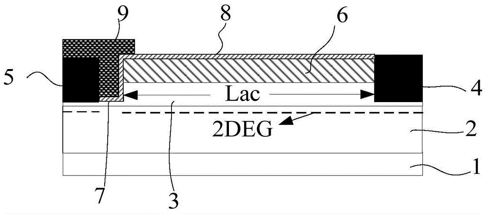
[0040] Figure 2-Figure 9 It is a schematic diagram of the manufacturing process steps of a gallium nitride heterojunction MIS power diode according to the present invention, and the process flow is as follows:

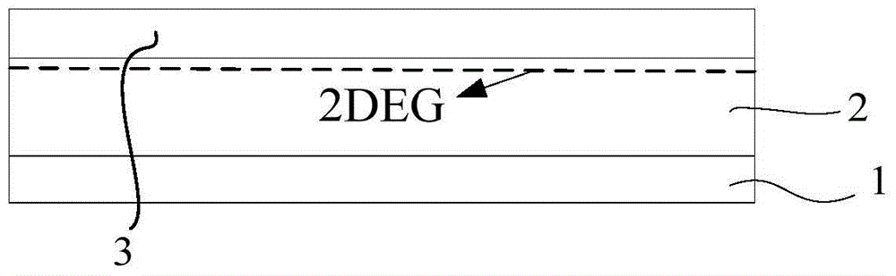
[0041] (1) Using metal-organic chemical vapor deposition or molecular beam epitaxy, a GaN layer 2 and a barrier layer AlXN layer 3 are sequentially grown on the substrate 1, such as figure 2 shown;

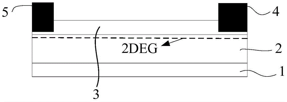
[0042] (2) Using photolithography technology, evaporate (or sputter) ohmic metal, and perform rapid thermal annealing to form the first ohmic contact metal 4 and the second ohmic contact metal 5, such as image 3 shown;

[0043] (3) Use ion implantation technology or dry etching mesa technology to form device-to-device isolation;

[0044] (4) Plasma-enhanced chemical vapor deposition is used to uniformly grow a passivation layer on the heterojunction barrier layer, such as Figure 4 shown. Using photolithography technology, the pattern of the groove area is photo-et...


PUM

PropertyMeasurementUnit
Thicknessaaaaaaaaaa
Thicknessaaaaaaaaaa

Abstract

The invention relates to the technical field of semiconductor devices, in particular to a gallium nitride heterojunction MIS grid-control power diode and a manufacturing method thereof. The gallium nitride heterojunction MIS grid-control power diode is characterized in that the two-dimensional electron gas below Schottky metal is exhausted by etching the barrier layer below the anode Schottky metal, insulating media and Schottky metal are precipitated in the etched groove to form a Schottky metal/insulting medium/semiconductor (MIS) grid-control structure, the MIS grid-control structure can control the on and off of a device and can effectively reduce the reverse leakage of the device and increase the reverse voltage resistance of the device; an Ohm/Schottky metal short-circuit mixed anode is formed at the anode of the diode, and low positive turning-on voltage of the device can be achieved. The gallium nitride heterojunction MIS grid-control power diode has the advantages of high reverse voltage resistance, high breakover currents, low turning-on voltage, low breakover resistance, low power consumption and the like. The manufacturing method is especially applicable to the gallium nitride heterojunction diode.

Description

technical field [0001] The invention relates to the technical field of semiconductor devices, in particular to a gallium nitride heterojunction MIS (Schottky metal / insulator / semiconductor) gate-controlled power diode and a manufacturing method thereof. Background technique [0002] As a typical representative of the third-generation wide-bandgap semiconductor, gallium nitride (GaN) has many excellent characteristics: high critical breakdown electric field (~3.5×10 6 V / cm), high electron mobility (~2000cm 2 / v·s), high two-dimensional electron gas (2DEG) concentration (~10 13 cm -2 ) and good high temperature working ability, etc. High electron mobility transistor (HEMT) based on AlGaN / GaN heterojunction (or heterojunction field effect transistor HFET, modulation doped field effect transistor MODFET, hereinafter collectively referred to as HEMT devices) has been applied in the semiconductor field, especially in The field of radio frequency / microwave has been applied in wi...

Claims


Application Information

Patent Timeline
IPC IPC(8): H01L29/872H01L29/739H01L29/40H01L29/06H01L29/45H01L21/28H01L29/66
CPCH01L29/7391H01L29/0684H01L29/40H01L29/401H01L29/407H01L29/454H01L29/66212H01L29/66219H01L29/66356H01L29/8725
Inventor 周琦陈博文靳旸李健鲍旭施媛媛汪玲陈万军张波
Owner UNIV OF ELECTRONIC SCI & TECH OF CHINA
Why Eureka
Try Eureka