Blue-fluorescence material and application thereof
A luminescent material and blue fluorescent technology, which is applied in the field of blue fluorescent luminescent materials, can solve the problems of few types of blue light materials and low device life, and achieve the effects of increasing photoelectric conversion efficiency, improving luminous performance, and increasing the number
- Summary
- Abstract
- Description
- Claims
- Application Information
AI Technical Summary
Problems solved by technology
Method used
Image
Examples
Embodiment 1
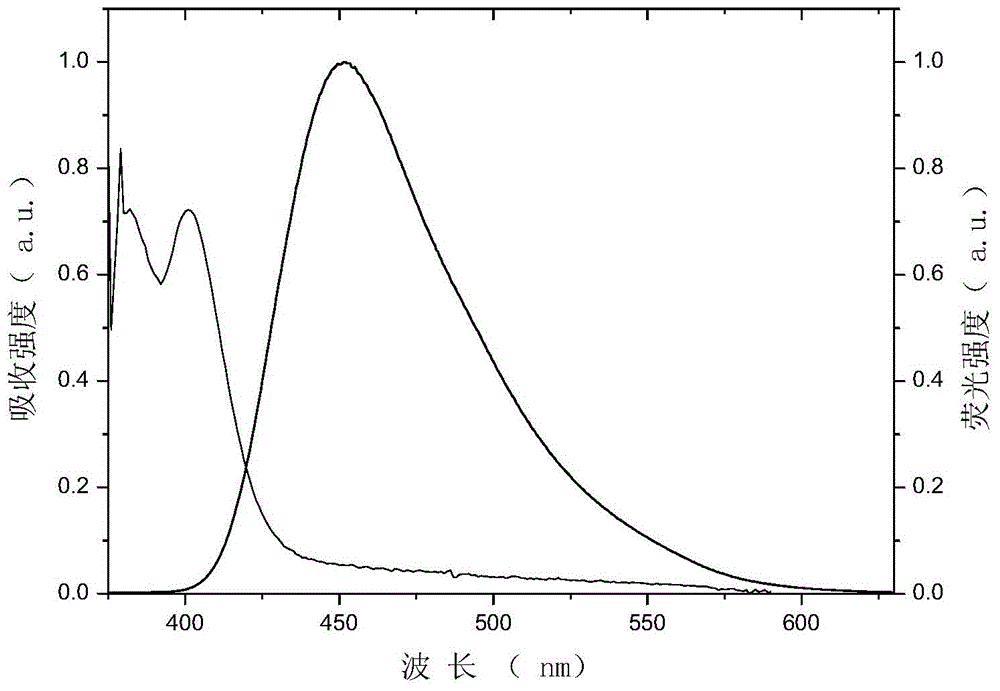
[0043] Example 1 Preparation of blue fluorescent luminescent material TPEPAnOMeCN
[0044] 1) 4-Bromo-4 , -Synthesis of Chlorobenzophenones
[0045]Add 4-bromobenzoic acid (10g, 0.05mol), dichloromethane (100ml), oxalyl chloride (8.18g, 0.065mol, 6ml) into the three-necked flask, stir at 25°C, and the system turns into a white cloudy liquid. Quickly drop 1-2 drops of N,N-dimethylformamide (DMF) into the system, and a large number of bubbles are observed, and the reaction is violent. Stir at 25°C for 30 minutes. Heating, the bath temperature was set to 45°C, the system became clear after 30 minutes of reaction, and the reaction was continued for 1.0 hours. To remove the solvent, measure 20ml of monochlorobenzene to dissolve the product after the solvent removal. Anhydrous aluminum trichloride (0.0575 mol, 7.58 g) was added in 3 portions. The bath temperature was set to 120°C, under nitrogen protection, a large amount of hydrochloric acid gas was generated during this period...
Embodiment 2
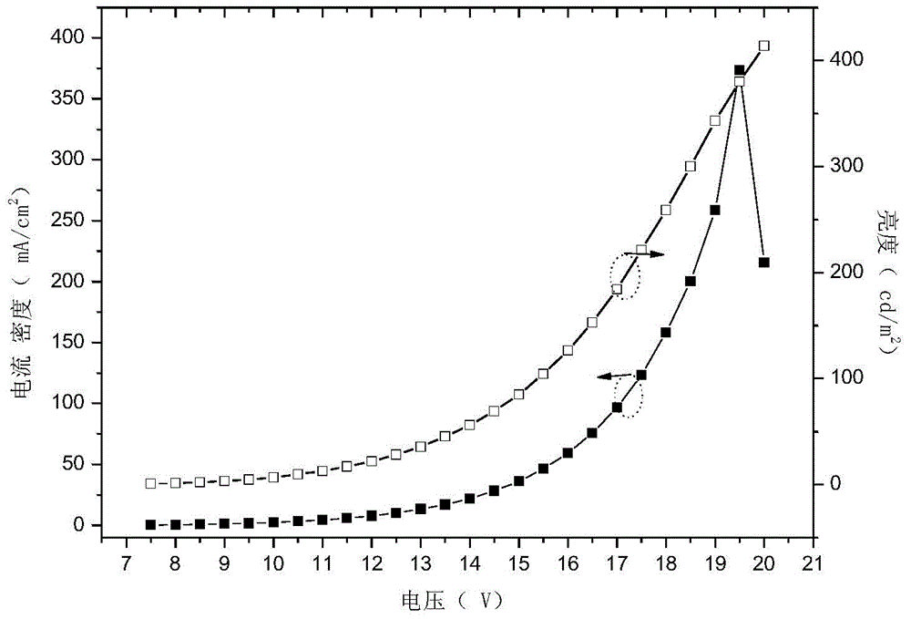
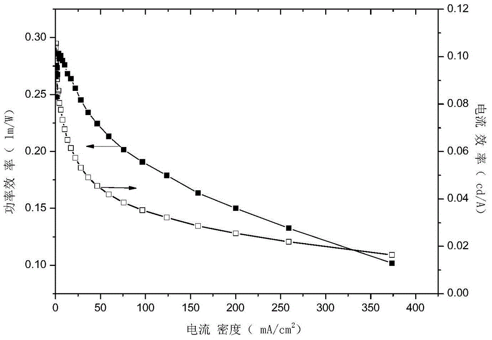
[0081] Example 2 Application of blue fluorescent luminescent material TPEPAnOMeCN in organic electroluminescent devices
[0082] This embodiment prepares organic electroluminescence device according to the following method:
[0083] a) Cleaning ITO (indium tin oxide) glass: ultrasonically clean the ITO glass with deionized water, acetone, and ethanol for 30 minutes each, and then treat it in a plasma cleaner for 15 minutes;
[0084] b) Vacuum evaporation of a hole transport layer NPB on the anode ITO glass with a thickness of 50nm;
[0085] c) On the hole transport layer NPB, vacuum evaporate the luminescent layer TPEPAnOMeCN with a thickness of 30nm;
[0086] d) On top of the light-emitting layer TPEPAnOMeCN, an electron transport layer TPBI is vacuum-evaporated with a thickness of 40 nm;
[0087] e) On the electron transport layer TPBI, the electron injection layer LiF is vacuum evaporated, with a thickness of 1 nm;
[0088] f) On the electron injection layer LiF, a catho...
Embodiment 3
[0090] Example 3 Application of blue fluorescent luminescent material TPEPAnOMeCN in organic electroluminescent devices II
[0091] This embodiment prepares organic electroluminescence device according to the following method:
[0092] a) Cleaning ITO (indium tin oxide) glass: ultrasonically clean the ITO glass with deionized water, acetone, and ethanol for 30 minutes each, and then treat it in a plasma cleaner for 15 minutes;
[0093] b) Vacuum evaporation or solution film-forming hole transport layer TAPC on the anode ITO glass, with a thickness of 50nm;
[0094] c) On top of the hole transport layer TAPC, vacuum evaporate the luminescent layer TPEPAnOMeCN with a thickness of 30nm;
[0095] d) On the light-emitting layer TPEPAnOMeCN, an electron transport layer TmPyPB is vacuum-evaporated with a thickness of 40 nm;
[0096] e) On top of the electron transport layer TmPyPB, an electron injection layer LiF is vacuum evaporated with a thickness of 1 nm;
[0097] f) On the el...
PUM
 Abstract
Description
Claims
Application Information


