Surface pretreatment method for reducing interface state density of SiC MOS

A technology of surface pretreatment and interface state density, applied in semiconductor/solid-state device manufacturing, electrical components, circuits, etc., can solve problems such as instability, inability to fundamentally solve surface state problems, and easy surface oxidation, so as to avoid damage. , The effect of reducing SiCMOS interface state density

Active Publication Date: 2016-02-24
DALIAN UNIV OF TECH
View PDF5 Cites 17 Cited by
  • Summary
  • Abstract
  • Description
  • Claims
  • Application Information

AI Technical Summary

Problems solved by technology

The boiling water treatment method is simple and effective, but its surface is easy to oxidize, and it is unstable at high temperature, and the passivation effect is obviously weakened after heat treatment above 400 °C
In addition, there are C and OH on the surface - and F - Ionic surface adsorption; use HCl:HF instead of traditional HF:H 2 After O, to a certain extent, it is beneficial to reduce the surface ion adsorption and improve the hydrogenation effect, but it cannot fundamentally solve the surface state problem, and cannot eliminate the remaining C on the surface after cleaning.
[0007] High-temperature hydrogen treatment is to anneal the

Method used


Image

  • Surface pretreatment method for reducing interface state density of SiC MOS
  • Surface pretreatment method for reducing interface state density of SiC MOS
  • Surface pretreatment method for reducing interface state density of SiC MOS

Examples


Embodiment 1

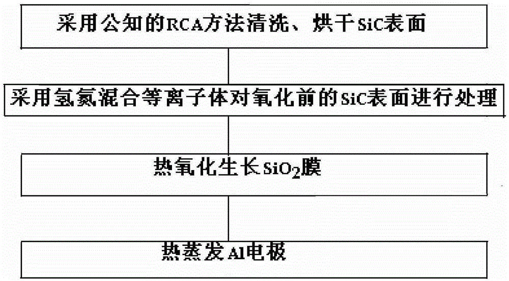
[0043] Such as figure 1 As shown, a surface pretreatment method for reducing the SiCMOS interface state density includes the following steps:

[0044] Step 1, using the known RCA method to clean and dry the SiC surface, specifically including the following sub-steps:

[0045] (a) Put SiC in a beaker, and use deionized water and ultrasonic cleaning several times until there is no obvious foreign matter;

[0046] (b) Wash with concentrated sulfuric acid, heat to 80°C, cook for 10 minutes, then soak for 30 minutes, add hydrogen peroxide and soak for 30 minutes, rinse the surface with deionized water several times;

[0047] (c) Using deionized water, H 2 o 2 , NH 4 OH mixed solution to clean, then wash with buffered hydrofluoric acid solution, and finally rinse the SiC surface several times with deionized water;

[0048] (d) using deionized water, H 2 o 2 , HCl mixed solution to clean, then wash with buffered hydrofluoric acid solution, and finally rinse the SiC surface sev...

Embodiment 2

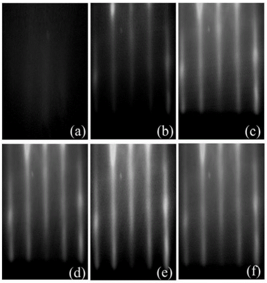
[0065] refer to figure 2 , although the RHEED image of the SiC surface cleaned by the traditional RCA method is in the form of linear stripes, the stripes are not clear and the contrast is poor, indicating that the atomic arrangement on the SiC surface is irregular and the single crystal orientation is poor. After hydrogen-nitrogen mixed plasma treatment, as the processing time increases, the RHEED image shows very clear linear stripes at 8 minutes, and the contrast is also very high, indicating that the SiC surface is clean, the atomic arrangement is regular, smooth, and the single crystal orientation is good. , and after calculation, the SiC surface treated by ECR hydrogen-nitrogen mixed plasma is approximately 1×1 structure, and no reconstruction occurs.

Embodiment 3

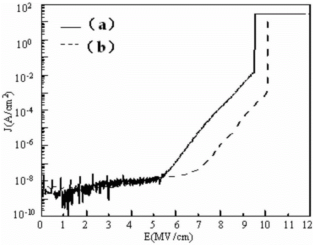
[0067] The SiCMOS capacitor device obtained by adopting the traditional method and the SiCMOS capacitor device obtained after the SiC surface is pretreated by the method of the present invention for 8 min are carried out, and the I-V characteristic test is carried out, and the Keithley4200 semiconductor parameter analyzer is used to complete the voltage scanning range. The length is 0.05V, and the hold time is 0.1s. The measured results are as image 3 As shown, compared with the SiCMOS capacitive device obtained by the traditional method and the method of the present invention, SiO 2 The breakdown field strengths of the films are 9.5MV / cm and 10.1MV / cm, and the barrier heights are 2.48eV and 2.74eV, respectively, indicating that the ECR hydrogen-nitrogen mixed plasma treatment improves SiO 2 insulating properties of the film.


PUM

PropertyMeasurementUnit
Breakdown field strengthaaaaaaaaaa

Abstract

The invention relates to the technical field of semiconductor device performance improvement. A surface pretreatment method for reducing the interface state density of SiC MOS comprises the following steps: (1) using a known RCA method to clean and dry the surface of SiC; (2) using a hydrogen-nitrogen hybrid plasma to treat the surface of SiC before oxidation; (3) growing an SiO2 film through thermal oxidation; and (4) thermally evaporating an Al electrode. According to the invention, a low-energy and high-activity low-temperature hydrogen-nitrogen hybrid plasma produced by an ECR microwave plasma system is adopted to pre-treat the surface of SiC before oxidation. A low-temperature process is realized, and damage to the surface of SiC by a conventional plasma is avoided. Moreover, hydrogen and nitrogen passivation effects are combined, impurity ions and residual carbon on the surface of SiC are removed effectively, hydrogen and nitrogen on the surface inhibit the generation of defects in the oxidation process, and the interface state density of SiC MOS is reduced significantly. In addition, the system is equipped with an RHEED in-situ monitoring system, and is especially suitable for SiC surface passivation process monitoring and mechanism research.

Description

technical field [0001] The invention relates to a surface pretreatment method for reducing SiCMOS interface state density, and belongs to the technical field of performance improvement of semiconductor devices. Background technique [0002] As a third-generation semiconductor material, SiC has a larger band gap, higher electron mobility, saturated electron velocity, and thermal conductivity than Si, making SiC more suitable for high-temperature, high-power power electronics. . At the same time, SiC is the only one that can be thermally oxidized to form SiO 2 The film is a wide bandgap compound semiconductor, which makes it possible for SiC-MOS devices to learn from the mature Si process. However, in actual production due to SiO 2 The high density of state states at the / SiC interface leads to low channel mobility, which seriously restricts the performance of SiC-MOS devices. Therefore, reducing the SiO 2 / SiC interface state density is a key technical issue in the resea...

Claims


Application Information

Patent Timeline
IPC IPC(8): H01L21/336H01L21/324
CPCH01L21/324H01L29/66409H01L2229/00
Inventor 王德君刘冰冰秦褔文
Owner DALIAN UNIV OF TECH
Why Eureka
Try Eureka