

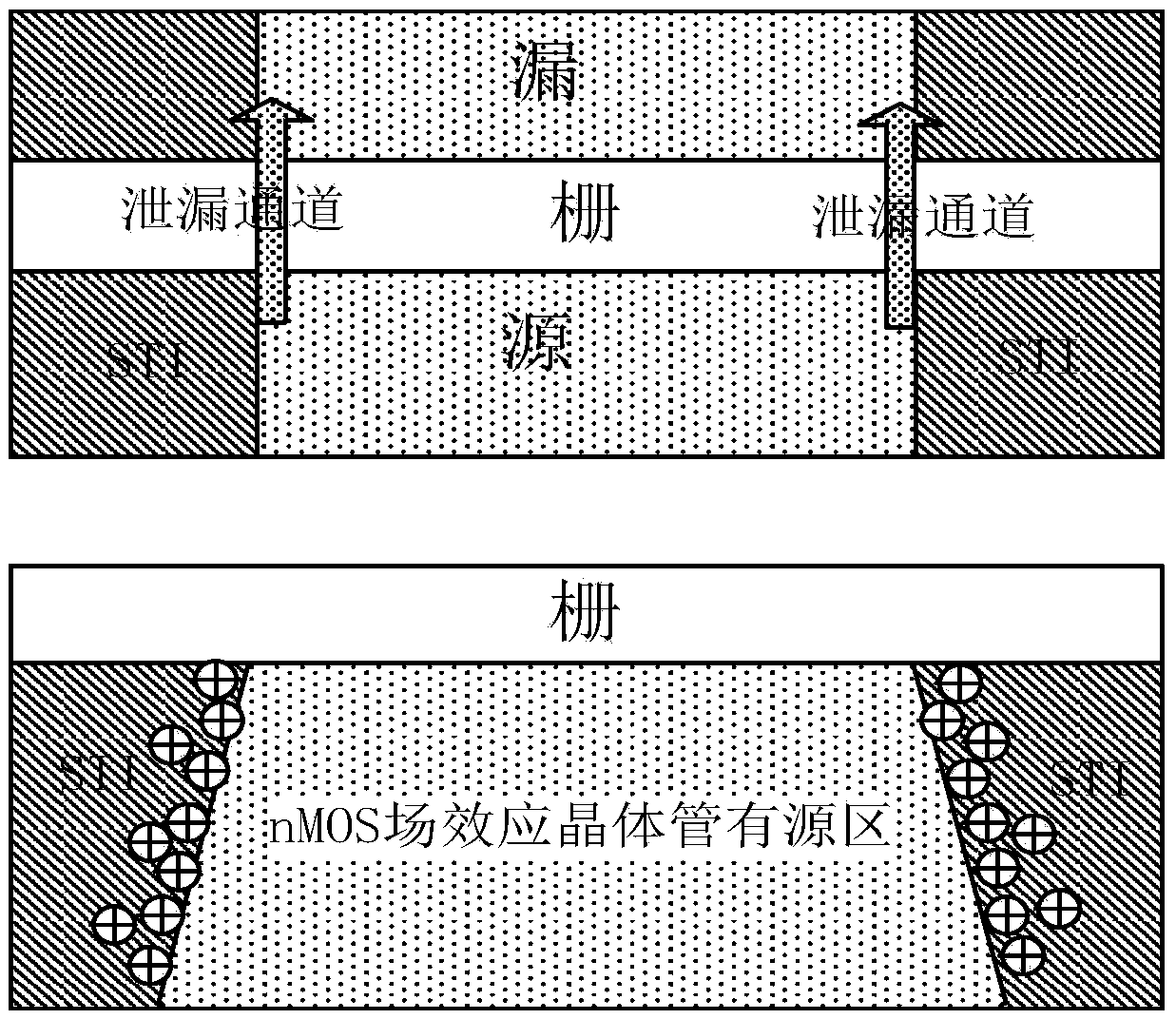
65nm technology-based super-steep reverse-doping radiation-proof MOS field-effect tube
A field effect transistor and reverse doping technology, which is applied in the direction of electrical components, electric solid devices, circuits, etc., can solve the problem of poor anti-radiation characteristics of nMOS field effect transistors, reduced threshold voltage of nMOS field effect transistors, and off-state leakage Current increase and other issues, to achieve the effect of improving the anti-radiation characteristics, improving the anti-radiation performance, and reducing the off-state leakage current
- Summary
- Abstract
- Description
- Claims
- Application Information
AI Technical Summary
Problems solved by technology
Method used
Image

Examples
example 1
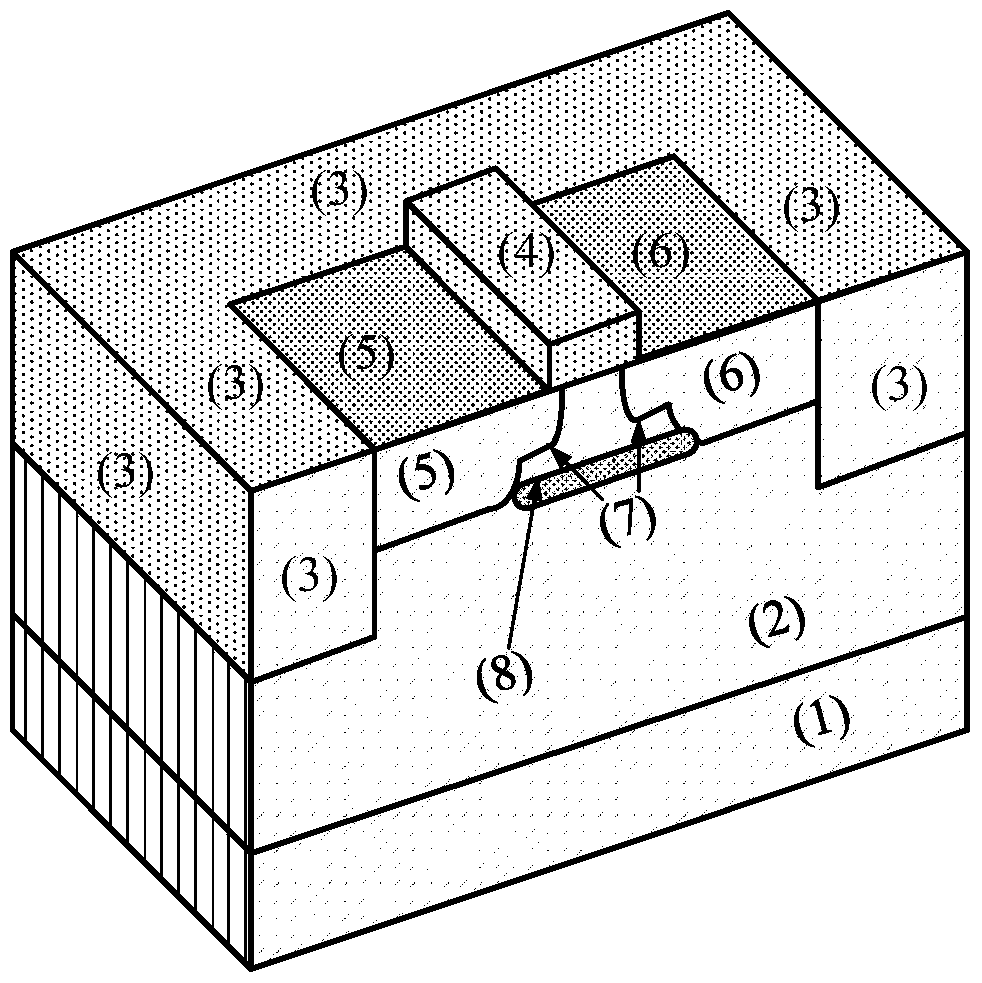
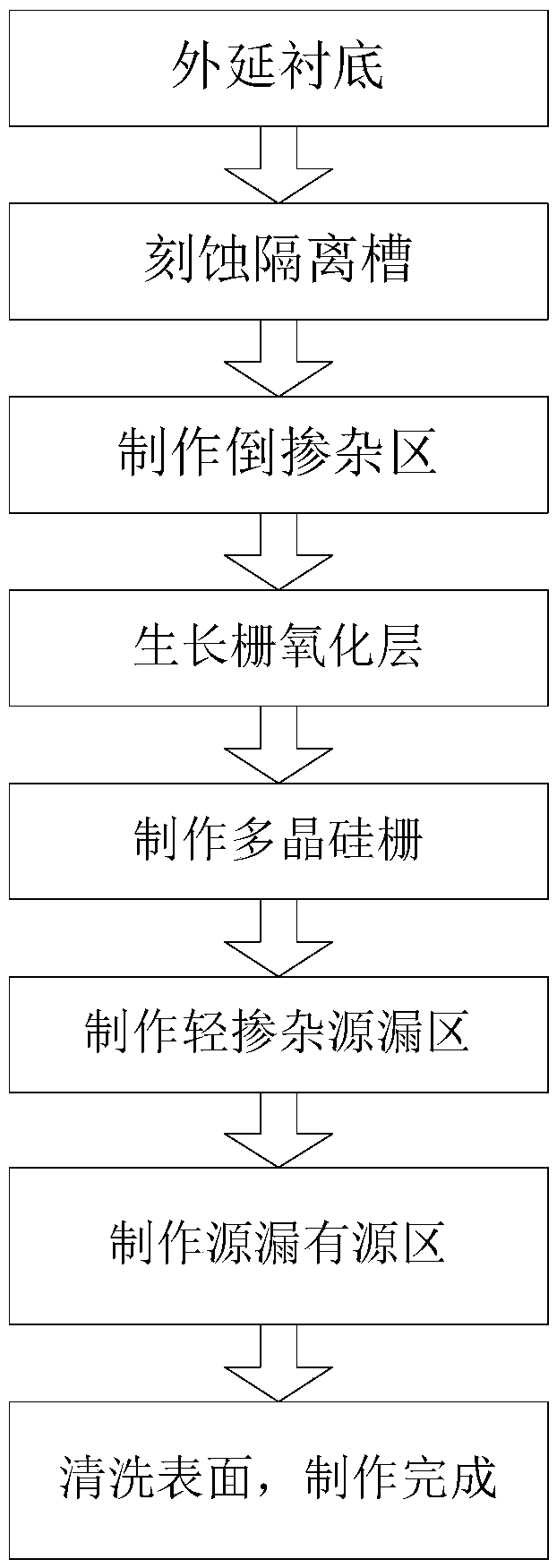
[0040] Example 1: Making a substrate with a doping concentration of 2×10 17 cm -3 , the doping concentration of the source and drain regions is 1×10 19 cm -3 , the diffusion length of the source and drain regions is 50nm, and the ultra-steep retrograde doping concentration is 6×10 17 cm -3 , a 65nm nMOS field effect transistor with an ultra-steep inverse doping depth of 58nm and an ultra-steep inversion length of 5nm.
[0041] Step 1, growing an epitaxial layer.
[0042] First use the method of chemical vapor deposition to SiH at a temperature of 650 °C 4 growing an epitaxial layer with a thickness of 600nm in the (100) crystal direction of the P-type Si substrate as a reactant;
[0043] Then doped with 2×10 by diffusion process 17 cm -3 The concentration of boron ions forms a p-type doped region with a depth of 100nm on the surface of the epitaxial layer to adjust the channel concentration.
[0044] Step 2, etching the isolation groove.
[0045] First grow thin SiO ...
example 2
[0076] Example 2: Making a substrate with a doping concentration of 5×10 17 cm -3 , the doping concentration of the source and drain regions is 3×10 19 cm -3 , the diffusion length of the source and drain regions is 55nm, the diffusion length of the source and drain regions is 50nm, and the ultra-steep retrograde doping concentration is 1×10 18 cm -3 , a 65nm nMOS field effect transistor with an ultra-steep inverse doping depth of 54nm and an ultra-steep inversion length of 20nm.
[0077] Step 1, growing an epitaxial layer.
[0078] 1.1) Using the chemical vapor deposition method at a temperature of 600 ° C to SiH 4 An epitaxial layer with a thickness of 800nm is grown on a P-type substrate as a reactant;
[0079] 1.2) Doping 5×10 by diffusion process 17 cm -3 The concentration of boron ions forms a p-type doped region with a depth of 150nm on the surface of the epitaxial layer to adjust the channel concentration.
[0080] Step 2, etching the isolation groove.
[0...
example 3
[0117] Example 3: Making a substrate with a doping concentration of 9×10 17 cm -3, the doping concentration of the source and drain regions is 5×10 19 cm -3 , the diffusion length of the source and drain regions is 60nm, and the ultra-steep retrograde doping concentration is 2×10 18 cm -3 , a 65nm nMOS field effect transistor with an ultra-steep inverse doping depth of 53nm and an ultra-steep inversion length of 27nm.
[0118] Step a, growing an epitaxial layer.
[0119] SiH was deposited at a temperature of 500 °C by chemical vapor deposition 4 An epitaxial layer with a thickness of 1000nm is grown on a P-type substrate as a reactant; doped with 9×10 17 cm -3 The concentration of boron ions forms a p-type doped region with a depth of 150nm on the surface of the epitaxial layer to adjust the channel concentration.
[0120] Step b, etching the isolation groove.
[0121] Thin SiO with a thickness of 5 nm was grown on the epitaxial layer by a dry oxygen oxidation process...
PUM
 Abstract
Description
Claims
Application Information