Vertically structured LED chip preparation method

A LED chip and vertical structure technology, which is applied in the direction of electrical components, circuits, semiconductor devices, etc., can solve the problems of complex vertical chip process, chip appearance deformation, gallium nitride material corrosion and other problems, so as to reduce the risk of unintentional conduction Possibility, improvement of product comprehensive yield, and effect of shortening etching process time

Inactive Publication Date: 2016-06-08
XI AN JIAOTONG UNIV
View PDF1 Cites 9 Cited by
  • Summary
  • Abstract
  • Description
  • Claims
  • Application Information

AI Technical Summary

Problems solved by technology

Compared with horizontal structure LED chips, since vertical structure LED chips need substrate stripping and transfer, electrode pattern processing, U-GaN gallium nitride material etching area definition, passivation protection layer, etc., the vertical chip process is relatively horizontal. chip complex
[0003] Due to the particularity of the product, the vertical structure chip must realize the complete division of the epitaxial layer material between single chips. At present, it is mostly realized by plasma dry deep etching or laser ablation aisle combined with high temperature wet etching. At the same time, in order to avoid Chips are affected by the impact of high-pressure gas generated at the moment of laser lift-off, and it is necessary to reserve a deep etching path or laser ablation and its buffer area with a width of more than 100um. out reduction
However, there are still other process problems and hidden dangers in the above technologies. For example, the dry deep etching process of gallium nitride takes a long time and has low productivity, and it is difficult to control the shape of the etched sidewall to obtain a trapezoidal sidewall structure. The collapse of the sidewall during etching can cause the appearance of the chip to deform and even cause leakage. Although the laser ablation and high-temperature wet etching process can solve the above sidewall shape control problem, due to the gallium nitride between the unit areas of the chip in the laser ablation process The material distance is still relatively close to about 7-20um (laser line width limit), and there is still a hidden danger of chip leakage caused by the impact of high-pressure gas generated at the moment of peeling off. When GaN material is used in a wide inactive area, since only one interface of the ablation channel opening is relatively small, it is easy to corrode the GaN material uncleanly, which may lead to chip leakage if the appearance is abnormal and severe.

Method used


Image

  • Vertically structured LED chip preparation method
  • Vertically structured LED chip preparation method

Examples


preparation example Construction

[0023] A kind of vertical structure LED chip preparation method of the present invention, comprises the following steps:

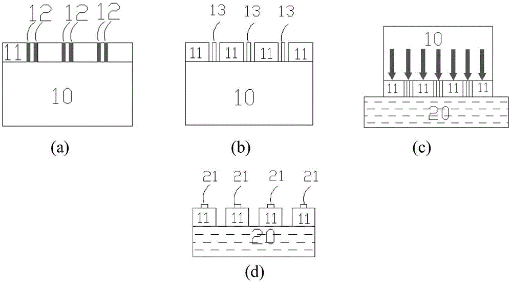
[0024] 1) Obtain an LED epitaxial layer 11 with an LED structure by using an epitaxial growth method on the heterogeneous substrate 10; wherein, the heterogeneous substrate 10 is made of sapphire, silicon or silicon carbide; the LED epitaxial layer 11 is made of GaN, AlN, Made of InGaN, AlGaN or AlInGaN materials.

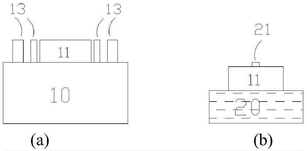
[0025] 2) On the upper surface of the LED epitaxial layer 11, a plurality of staggered grooves 12 are processed by laser to form a columnar surrounding gallium nitride high-pressure gas release sacrificial region 13; wherein, the number of the multi-channel staggered grooves is greater than or equal to 2, using Non-positioning blind scribing or positioning scribing based on the flat edge of the wafer, its surrounding shape is a regular or irregular vertical chip graphic outline according to the design requirements, the multiple staggered groove...

Embodiment 1

[0031](1) Firstly, the epitaxial material layer 11 of the gallium nitride system LED is prepared on the heterogeneous substrate 11 by epitaxial method. , multiple quantum well MQW, electron blocking layer EBL, heavily doped P-GaN, its thickness is controlled at 5-6 microns, the heterogeneous substrate includes but not limited to sapphire, silicon, silicon carbide, or various types of high temperature resistant and A support substrate with a transition layer that matches the lattice of the III-N material, the preferred solution is a sapphire substrate, and the epitaxial layer includes the LED epitaxial structure composed of GaN / AlN / InGaN / AlGaN / AlInGaN and other material systems One or more, the preferred solution is GaN / InGaN;

[0032] (2) On the epitaxial layer 11 of the LED wafer, a layer of silicon oxide or silicon nitride material protective layer is prepared by PECVD, and grooves are processed on the gallium nitride surface by using an equal-spaced laser scribing method, a...

Embodiment 2

[0037] The general process is the same as in Example 1, the difference is that when laser scribing is performed to prepare the columnar high-pressure gas surrounding GaN to release the sacrificial region, multiple channels of laser processing with unequal spacing are used to form multi-layer high-pressure gas surrounding GaN columnarly with unequal spacing. Release the sacrificial area, the number of layers is greater than or equal to 2, using the unequal spacing area, effectively relieve the high-pressure gas impact at the moment of stripping, and provide more contact interfaces for high-temperature wet etching, and at the same time, the edge of the outermost scribe line in the columnar area The distance from the edge of the effective area of ​​the adjacent vertical chip is not less than ten microns, and then the chip manufacturing process is the same as that of Embodiment 1, and finally the vertical structure LED chip preparation is completed.

[0038] The invention adopts hi...


PUM


Abstract

The invention discloses a vertically structured LED chip preparation method. The method comprises the steps of 1) obtaining an LED epitaxial layer of an LED structure on a heterogeneous substrate according to the epitaxial growth method; 2) forming multiple interlaced grooves on the upper surface of the LED epitaxial layer through the laser machining process so as to form a cylindrically surrounded gallium nitride high-pressure gas release sacrificial region; 3) successively preparing an ohmic contact layer and a first bonding material layer on the LED epitaxial layer, and preparing a second bonding material layer on a bonding substrate; 4) bonding the first bonding material layer on the LED epitaxial layer and the second bonding material layer on the bonding substrate together, and removing the heterogeneous substrate through the laser lift-off process; 5) etching the lifted-off LED epitaxial layer onto an N-GaN surface, removing the gallium nitride material outside the cylindrically surrounded gallium nitride high-pressure gas release sacrificial region and the effective region of the LED epitaxial layer based on the wet etching technology, and finally completing the preparation of a passivation layer and an N electrode. In this way, a vertically structured LED chip can be obtained.

Description

Technical field: [0001] The invention belongs to the technical field of light-emitting diodes, in particular to the field of preparing vertical-structure LED chips based on laser lift-off technology. Background technique: [0002] Since the LED white light lighting technology entered a rapid development stage in the 1990s, the LED application market has exceeded hundreds of billions of yuan. At the same time, with the rapid development of AlGaN ultraviolet LED / LD devices in the past two years, it has Application fields such as sterilization and semiconductor solid-state lasers also show good market development prospects. The most common LED products adopt a horizontal structure design, the current flows through the light-emitting area of ​​the LED in the horizontal direction, and electrons are injected laterally from one electrode to the other, resulting in uneven distribution of current density on the way, resulting in current congestion effect resulting in uneven luminesce...

Claims


Application Information

Patent Timeline
Patent Type & Authority Applications(China)
IPC IPC(8): H01L33/00
CPCH01L33/007
Inventor 云峰郭茂峰
Owner XI AN JIAOTONG UNIV
Why Eureka
Try Eureka