Method for preparing orderly one-dimensional nanometer array on conductive substrate
A conductive substrate and nano-array technology, applied in the direction of nano-technology, can solve the problems such as the reduction of the order degree of porous alumina, and achieve the effect of facilitating subsequent applications and being convenient to hold
- Summary
- Abstract
- Description
- Claims
- Application Information
AI Technical Summary
Problems solved by technology
Method used
Image

Examples
Embodiment 1
[0065] This embodiment is used for illustrating and adopts the method for the present invention to prepare metallic nickel nanorod, comprises the following steps:
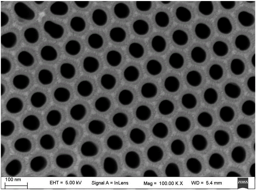
[0066] S1: Prepare a through-hole anodized aluminum template with a thickness of 800nm, and the surface scanning electron microscope (SEM) of the prepared through-hole anodized aluminum template is as follows figure 1 As shown, the through-hole anodized aluminum template has highly ordered nanopores, and the preparation of the through-hole anodized aluminum template specifically includes the following steps:
[0067] S11: Synthesis of porous anodized aluminum by two-step anodizing method using aluminum foil;
[0068] S12: peel off the aluminum substrate after applying a layer of nail polish on the porous anodized aluminum surface;
[0069] S13: Soak the porous anodized aluminum in a phosphoric acid solution with a mass fraction of 5% for 40 minutes to remove the barrier layer, then soak the porous anodized aluminu...
Embodiment 2
[0076] This embodiment is used to illustrate adopting the method of the present invention to prepare cadmium selenide semiconductor nanowires, comprising the following steps:
[0077] S1: Prepare a through-hole anodized aluminum template with a thickness of 900nm, wherein the preparation of the through-hole anodized aluminum template specifically includes the following steps:
[0078] S11: Synthesis of porous anodized aluminum by two-step anodizing method using aluminum foil;
[0079]S12: After coating a layer of polydimethylsiloxane (PDMS) on the porous anodized aluminum surface, the aluminum substrate is peeled off;
[0080] S13: Soak porous anodized aluminum in a phosphoric acid solution with a mass fraction of 3% for 50 minutes to remove the barrier layer, then soak porous anodized aluminum in acetone for 20 minutes to remove polydimethylsiloxane (PDMS) Obtain through-hole anodized aluminum template;
[0081] S14: Soak the through-hole anodized aluminum template in hydro...
Embodiment 3
[0087] This embodiment is used to illustrate adopting the method for preparing silver nanowires of the present invention, comprises the following steps:
[0088] S1: Prepare a through-hole anodized aluminum template with a thickness of 400nm, wherein the preparation of the through-hole anodized aluminum template specifically includes the following steps:
[0089] S11: Synthesis of porous anodized aluminum by two-step anodizing method using aluminum foil;
[0090] S12: peel off the aluminum substrate after applying a layer of nail polish on the porous anodized aluminum surface;
[0091] S13: Soak the porous anodized aluminum in a phosphoric acid solution with a mass fraction of 8% for 40 minutes to remove the barrier layer, then soak the porous anodized aluminum in acetone for 15 minutes to remove the nail polish to obtain a through-hole anodized aluminum template;
[0092] S14: Soak the through-hole anodized aluminum template in hydrogen peroxide with a mass fraction of 30% f...
PUM
| Property | Measurement | Unit |
|---|---|---|
| Thickness | aaaaa | aaaaa |
Abstract
Description
Claims
Application Information
 - Generate Ideas
- Intellectual Property
- Life Sciences
- Materials
- Tech Scout
- Unparalleled Data Quality
- Higher Quality Content
- 60% Fewer Hallucinations
Browse by: Latest US Patents, China's latest patents, Technical Efficacy Thesaurus, Application Domain, Technology Topic, Popular Technical Reports.
© 2025 PatSnap. All rights reserved.Legal|Privacy policy|Modern Slavery Act Transparency Statement|Sitemap|About US| Contact US: help@patsnap.com