Double-split groove gate charge storage type IGBT and manufacturing method thereof

A charge storage and charge storage layer technology, applied in semiconductor/solid-state device manufacturing, circuits, electrical components, etc., can solve problems such as the compromise characteristics affecting the switching loss of the device, increasing the gate capacitance, and increasing the switching loss of the device.

Active Publication Date: 2016-09-07
UNIV OF ELECTRONICS SCI & TECH OF CHINA
View PDF4 Cites 28 Cited by
  • Summary
  • Abstract
  • Description
  • Claims
  • Application Information

AI Technical Summary

Problems solved by technology

However, for the CSTBT device structure, due to the existence of a higher doping concentration and a certain thickness of the N-type charge storage layer, the breakdown voltage of the device is significantly reduced. In order to effectively shield the adverse effects of the N-type charge storage layer to obtain a certain device withstand voltage , it is necessary to adopt: 1) deep trench gate depth, so that the depth of the trench gate is greater than the junction depth of the N-type charge storage layer, but the deep trench gate depth not only increases the gate-emitter capacitance, but also increases Therefore, the switching speed of the device is reduced, the switching loss of the device is increased, and the compromise characteristics of the conduction voltage drop and switching loss of the device are affected; 2) the small cell width makes the channel The distance between the trench gates should be reduced as much as possible. However, the high-density trench MOS structure not only increases the gate capacitance of the device, but also reduces the switching speed of the device, increases the switching loss of the device, and affects the conduction of the device. The trade-off characteristics of on-voltage drop and switching loss, and increase the saturation current density of the device, making the short-circuit safe working area of ​​the device worse

Method used


Image

  • Double-split groove gate charge storage type IGBT and manufacturing method thereof
  • Double-split groove gate charge storage type IGBT and manufacturing method thereof
  • Double-split groove gate charge storage type IGBT and manufacturing method thereof

Examples


Embodiment 1

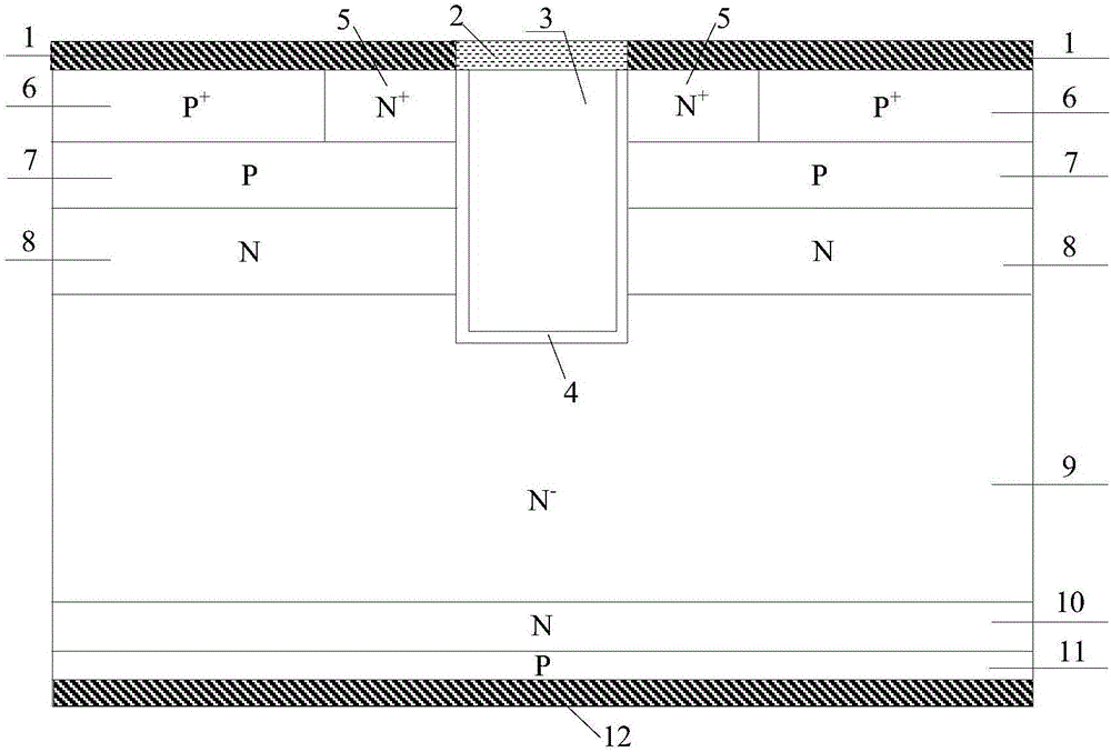
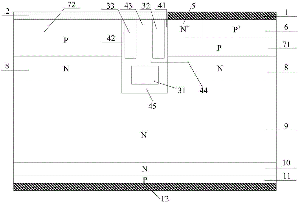
[0049] In this example, a double-split trench gate charge storage type IGBT, its cell structure is as follows figure 2As shown, it includes: the back collector metal 12, the P-type collector region 11 located on the back collector metal 12 and connected to it, the N-type field stop layer 10 located on the P-type collector region 11 and connected to it, The N-drift region 9 located on the N-type field stop layer 10 and connected to it; the compound double-split trench structure located in the middle of the upper part of the N-drift region 9 and connected to it; located on both sides of the upper part of the N-drift region 9 and connected to it The N-type charge storage layer 8, the sidewall of the N-type charge storage layer 8 is connected to the compound double split trench structure, and the p-type body regions 71 and 72 located on the upper part of the N-type charge storage layer 8 and connected thereto, so The sidewalls of the p-type body regions 71 and 72 are connected to...

Embodiment 2

[0051] In this example, a double-split trench gate charge storage type IGBT, its cell structure is as follows image 3 As shown, different from Embodiment 1, the lower part of the side split electrode 33 directly extends to the upper surface of the bottom split electrode 31, so that the side split electrode 33 and the bottom split electrode 31 are directly connected to further reduce the gate capacitance of the device.

Embodiment 3

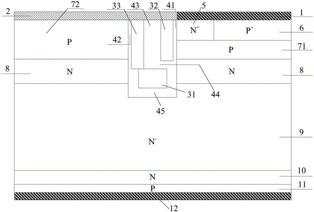
[0053] A double-split trench gate charge storage type IGBT of this example is different from Embodiments 1 and 2 in that the N-type charge storage layer 8 exists only in the lower part of the p-type body region 71, and the p-type body The junction of the region 72 is deeper than the fifth dielectric layer 45, and extends laterally to the lower part of the fifth dielectric layer 45 to further improve the concentration of the electric field at the bottom of the trench, and improve the breakdown voltage and reliability of the device.

[0054] The specific implementation scheme of the process manufacturing method of the present invention is illustrated by taking the double-split trench gate charge storage type IGBT with a voltage level of 600V as an example, and the specific process manufacturing method is as follows:

[0055] Step 1: Select a doping concentration of 2×10 14 A lightly doped FZ silicon wafer with a thickness of 300-600 microns per cm3 is used to form the N-drift re...


PUM


Abstract

The invention belongs to the technical field of a power semiconductor device and specifically relates to a groove gate charge storage type IGBT (insulated gate bipolar transistor). The bottom and side surfaces of a gate electrode in a groove of the device are provided with a double-split electrode equipotential with an emitter and a dielectric layer between the double-split electrode and the gate electrode, so that under the condition of not influencing threshold voltage and turning on of the IGBT device, grid capacitance is reduced, switching speed of the device is improved, and switching loss of the device is reduced; and meanwhile, the side-surface split electrode and a floating p-type base region at one side of the side-surface split electrode improve short circuit safety operation area of the device and carrier concentration distribution of the whole N drifting region, thereby improving performance and reliability of the device. The double-split groove gate charge storage type IGBT manufacturing method does not need extra processing steps, and is compatible with a conventional CSTB manufacturing method.

Description

technical field [0001] The invention belongs to the technical field of power semiconductor devices, and relates to an insulated gate bipolar transistor (IGBT), in particular to a trench gate charge storage type insulated gate bipolar transistor (CSTBT). Background technique [0002] Insulated Gate Bipolar Transistor (IGBT) is a new type of power electronic device combining MOS field effect and bipolar transistor. It not only has the advantages of easy driving and simple control of MOSFET, but also has the advantages of low conduction voltage of power transistor, large on-state current and small loss. It has become one of the core electronic components in modern power electronic circuits and is widely used in Various fields of the national economy such as communications, energy, transportation, industry, medicine, household appliances and aerospace. The application of IGBT plays an extremely important role in improving the performance of power electronic systems. [0003] S...

Claims


Application Information

Patent Timeline
Patent Type & Authority Applications(China)
IPC IPC(8): H01L29/06H01L29/40H01L29/739H01L21/28H01L21/331
CPCH01L29/0653H01L29/404H01L29/407H01L29/66348H01L29/7397H01L29/7398
Inventor 张金平廖航刘玮琪刘竞秀李泽宏任敏张波
Owner UNIV OF ELECTRONICS SCI & TECH OF CHINA
Why Eureka
Try Eureka