

A method for planarizing the optical surface of potassium dihydrogen phosphate crystal
A technology of potassium dihydrogen phosphate and optical surfaces, applied in chemical instruments and methods, crystal growth, single crystal growth, etc., can solve problems such as low-frequency error, high-quality processing difficulties, and affecting optical engineering effects, and achieve suppression of medium and high frequencies error, avoid low frequency error, good mechanical properties
- Summary
- Abstract
- Description
- Claims
- Application Information
AI Technical Summary
Problems solved by technology
Method used
Image

Examples
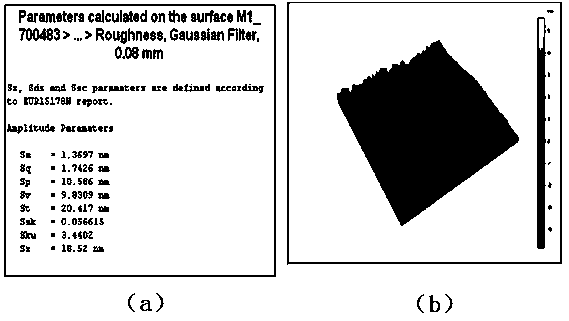
Embodiment 1
[0049] Including the following steps: (1) First use a single-point diamond lathe to measure 50×50×10mm 3 The Class I KDP crystal sample 1 was turned;
[0050] (2) Taking the sample 1 that has undergone single-point diamond turning as the processing object, and sputtering and depositing a layer of silicon film on the surface of the sample 1 by means of ion beam sputtering deposition; the target material of the film is silicon, and the target material is Specifications: 536×114×10.5mm;
[0051] Sputtering deposition time: 1h The main process parameters of planarization are controlled as follows:
[0052] Ion beam voltage 500V, ion beam current 150mA;
[0053] The ion beam accelerating voltage is 300V, and the ion beam accelerating current is 100mA;
[0054] Working gas: argon Gas flow rate: 35sccm;
[0055] Working pressure: 5.71E-2Pa ion beam incident angle 45°;
[0056] (3) Obtain a planarized layer by vacuum cooling, vacuum cooling: temperature 25°C, time 4h.
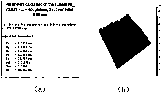
[0057] s...
Embodiment 2
[0062] Include the following steps:
[0063] (1) First use a single-point diamond lathe to cut to a size of 50×50×10mm 3 The Class I KDP crystal sample 2 was turned;
[0064] (2) Taking the sample 2 that has undergone single-point diamond turning as the processing object, use the method of ion beam sputtering to deposit a thin film on the surface of the sample 2 to sputter and deposit a layer of silicon film, the target specification: 536×114×10.5mm , the main process parameters of planarization are controlled as:
[0065] Ion beam voltage 500V, ion beam current 150mA;
[0066] The ion beam accelerating voltage is 300V, and the ion beam accelerating current is 100mA;
[0067] Working gas: Argon Gas flow rate: 35sccm;
[0068] Working pressure: 5.71E-2Pa, ion beam incident angle 45°, sputter deposition time 1.5h;
[0069] (3) Obtain a planarized layer by vacuum cooling. Vacuum cooling: temperature 25°C, time 4h.
[0070] see image 3 , Figure 4 , using Talysurf CCI-20...
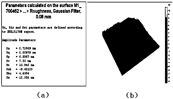
Embodiment 3
[0075] Include the following steps:
[0076] (1) First use a single-point diamond lathe to size 50×50×10mm 3 The Class I KDP crystal sample 3 was turned;
[0077] (2) Taking the sample 3 that has undergone single-point diamond turning as the processing object, use the method of ion beam sputtering to deposit a thin film on the surface of the sample 3 to sputter and deposit a layer of silicon film; target specification: 536×114×10.5 mm;
[0078] (3) Obtain a planarized layer by vacuum cooling.
[0079] The main process parameters of planarization are controlled as follows:
[0080] Ion beam voltage 500V, ion beam current 150mA;
[0081] The ion beam accelerating voltage is 300V, and the ion beam accelerating current is 100mA;
[0082] Working gas: Argon Gas flow rate: 35sccm;
[0083] Working pressure: 5.71E-2Pa ion beam incident angle 45°;
[0084] Sputtering deposition time 2h;
[0085] Vacuum cooling: temperature 25°C, time 4h.
[0086] see Figure 5 , Figure 6 ,...
PUM
| Property | Measurement | Unit |
|---|---|---|
| surface roughness | aaaaa | aaaaa |
| surface roughness | aaaaa | aaaaa |
Abstract
Description
Claims
Application Information