Three-dimensional carbon nano-material field effect flexible force sensing element and preparation method
A carbon nanomaterial and sensing element technology, applied in the field of electronic information, can solve the problems of environmental noise suppression, low signal-to-noise ratio, uncertainty of quantitative load measurement, etc., and achieve the effect of high sensitivity
- Summary
- Abstract
- Description
- Claims
- Application Information
AI Technical Summary
Problems solved by technology
Method used
Image

Examples
preparation example Construction
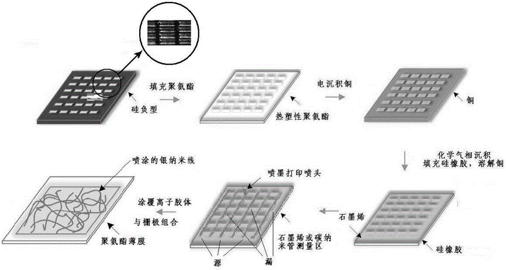
[0055] The preparation method of the three-dimensional structure of the copper surface first prepares the three-dimensional structure of thermoplastic polyurethane with the template method, and the steps are:
[0056] (1) First, single or multiple strip-shaped windows are etched on the surface of the silicon wafer with an oxide layer, and then the oxide layer is removed by HF etching, and then the pyramid is etched out with tetramethylammonium hydroxide aqueous solution and isopropanol Negative type of strip corrosion pit;
[0057] (2) Fill the above-mentioned pyramid-shaped silicon negative type of heating with molten thermoplastic polyurethane, and mechanically peel off after curing under vacuum to form a positive type polyurethane film;
[0058] (3) Coating one deck of polymethyl methacrylate with the glue-spinning method on the above-mentioned polyurethane positive surface, the thickness is less than 1 micron, after fully drying, evaporate one deck of pure copper on its su...
Embodiment 1
[0067] 1. Prepare single or multiple parallel photoresists with a width of 20 microns to 150 microns and a length of 150 microns to 500 microns on a single crystal silicon wafer with an oxide layer thickness of 500 nanometers and a crystal orientation of by photolithography For the window, use hydrofluoric acid to dissolve the oxide layer at the window, then place it in a 1:1 mixed solution of 25% by weight tetramethylammonium hydroxide solution and isopropanol, and corrode it at 95°C until the tapered tip is fully Take it out when it is formed, and get the silicon pyramid negative type after cleaning and drying;
[0068] 2. Cover a thermoplastic polyurethane sheet with a thickness of 2 mm on the negative surface of the silicon pyramid, heat it to 165°C in a vacuum, keep it under pressure for 5 minutes, take it out, peel off the polyurethane adhesive layer after cooling and solidification, and obtain a positive polyurethane elastomer film ;
[0069] 3. Soak the film positive...
Embodiment 2
[0079] 1, with embodiment one, 1;
[0080] 2, with embodiment one, 2;
[0081] 3. Coating a layer of semiconducting carbon nanotubes on the polyurethane elastomer film with the glue-spinning method, the carbon nanotubes are dispersed in the toluene solution, the concentration is 0.02mg / ml, and the thickness of the carbon nanotube film dispersed on the surface of the pyramid No more than 10 nanometers, dry at 140°C for 1 hour;
[0082] 4, with embodiment one, 8;
[0083] 5, with embodiment one, 9;
[0084] 6, with embodiment one, 10;
[0085] 7, with embodiment one, 11.
PUM
| Property | Measurement | Unit |
|---|---|---|
| Thickness | aaaaa | aaaaa |
| Thickness | aaaaa | aaaaa |
Abstract
Description
Claims
Application Information
 - Generate Ideas
- Intellectual Property
- Life Sciences
- Materials
- Tech Scout
- Unparalleled Data Quality
- Higher Quality Content
- 60% Fewer Hallucinations
Browse by: Latest US Patents, China's latest patents, Technical Efficacy Thesaurus, Application Domain, Technology Topic, Popular Technical Reports.
© 2025 PatSnap. All rights reserved.Legal|Privacy policy|Modern Slavery Act Transparency Statement|Sitemap|About US| Contact US: help@patsnap.com