
P-type gallium oxide doped film and preparation method thereof
A technology of gallium oxide and thin film, applied in the field of p-type doped gallium oxide thin film and its preparation, to achieve the effect of shortening the energy difference, increasing the net concentration, and improving the mobility
- Summary
- Abstract
- Description
- Claims
- Application Information
AI Technical Summary
Problems solved by technology
Method used
Image

Examples
Embodiment 1
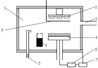
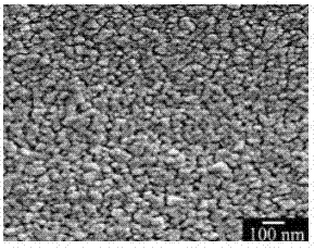
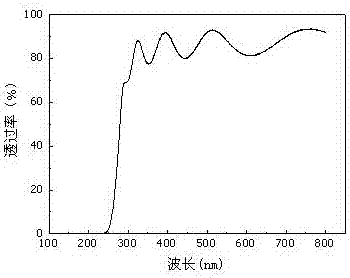
[0026] figure 1A schematic diagram of a p-type doped gallium oxide thin film preparation device designed for the present invention, a substrate holder 2 and a target groove 4 are arranged in the vacuum chamber 1 of the device schematic diagram, and a rotatable The baffle 9, the vacuum chamber 1 is evacuated through the exhaust system 3, and the target groove 4 is connected with the radio frequency matching device 8 and the radio frequency power supply 7. The elemental powder of the equivalent state element is placed in the evaporation source 6, and the vapor pressure of the equivalent state element is regulated by changing the temperature of the evaporation source 6. The substrate is installed on the substrate holder 2, the sputtering target is installed in the target groove 4, the sputtering gas argon enters the vacuum chamber 1 through the argon inlet 5, and the argon gas loads the vapor of the equivalent element into the glow discharge region, which increases the activity ...
Embodiment 2
[0032] The p-type doped gallium oxide film preparation device used in this example is the same as that in Example 1. Specifically, the preparation of a zinc-selenium co-doped gallium oxide film includes the following steps:
[0033] (1) Fully mix gallium oxide powder with a purity of 99.99% and zinc oxide powder with a purity of 99.99% at a weight ratio of 93:7, and press it into an embryo body of Φ60mm-4mm under a pressure of 65MPa. The pressing time is 20 minutes, and it is sent into High-temperature sintering furnace, sintering in air at 1300°C for 900 minutes, and sintering into zinc-doped gallium oxide ceramic targets.
[0034] (2) Install the cleaned n-type gallium oxide substrate on the substrate holder 2 in the vacuum chamber 1, install the zinc-doped gallium oxide ceramic target in the target groove 4 in the vacuum chamber 1, and adjust the target and substrate The bottom distance is 75 mm, and the equivalent element elemental selenium powder is placed in the evaporat...
Embodiment 3
[0037] The p-type doped gallium oxide film preparation device used in this example is the same as that in Example 1. Specifically, the preparation of a zinc-tellurium co-doped gallium oxide film includes the following steps:
[0038] (1) Fully mix the gallium oxide powder with a purity of 99.99% and the zinc oxide powder with a purity of 99.99% at a weight ratio of 94:6, and press it into a Φ60mm-4mm embryo body under a pressure of 60MPa. The pressing time is 25 minutes, and the High-temperature sintering furnace, sintering in air at 1350°C for 800 minutes, and sintering into zinc-doped gallium oxide ceramic targets.
[0039] (2) Install the cleaned sapphire substrate on the substrate holder 2 in the vacuum chamber 1, install the zinc-doped gallium oxide ceramic target in the target groove 4 in the vacuum chamber 1, and adjust the distance between the target and the substrate as 75 mm, put the equivalent element elemental tellurium powder in the evaporation source 6 . Vacuumi...
PUM
 Abstract
Description
Claims
Application Information