Metal catalytic texturing method for decreasing reflectance of polycrystalline silicon wafer cut with diamond wire

A diamond wire cutting, polycrystalline silicon wafer technology, applied in chemical instruments and methods, crystal growth, post-processing details, etc., can solve the problems of reducing reflectivity, corroding texture structure, high concentration, and achieving increased reactivity and low reflection. The effect of high efficiency and good compatibility

Inactive Publication Date: 2017-10-20
NANJING NAXIN NEW MATERIAL
View PDF6 Cites 26 Cited by
  • Summary
  • Abstract
  • Description
  • Claims
  • Application Information

AI Technical Summary

Problems solved by technology

The polysilicon textured sheet prepared by this method has a low reflectivity, which has laid a necessary foundation for further improving the photoelectric conversion efficiency, but the preparation process of this method is complicated, the cost of equipment and loss is expensive, and sulfuration will be emitted during the process. substances, halogen compounds, etc., especially Cl 2 , the gas is highly toxic and will pollute the environment
[0005] Patent No. 201610310040.5 discloses a diamond wire-cut polysilicon wafer texturing method using HF-HNO 3 -H 2 O Two-step texturing process, first use the traditional HF-HNO 3 -H 2 The O texturing system etches micron-scale larger wormhole structures on the surface of diamond-wire-cut polysilicon, and then uses H 2 o 2 -HF-H 2 The O system etches a micro-hole structure with a smaller size, and reduces the reflectivity of the silicon wafer surface through two-step acidity, but this texturing process cannot obtain a textured structure with uniform corrosion on the entire surface, and micron-sized insects on the surface of the textured surface Etching a smaller-sized micro-hole structure on the hole structure will also cause too many recombination centers to be formed on the surface of the silicon wafer, which is detrimental to improving the photoelectric performance of the battery
[0006] In recent years, some manufacturers have also tried to reduce the reflectivity of diamond wire-cut polysilicon wafers by wet chemical methods of metal ion assisted etching of polysilicon. For example, in the application number 201410652553.5, in the traditional HF-HNO 3 -H 2 O acidic system forms micro-textured surface after texturing, and then deposits metal nanoparticles on the micro-textured surface, and then puts it in an etching solution for etching to obtain a polycrystalline silicon wafer with a micro-nano composite textured structure. Metal-catalyzed chemical etching The etching adopts a two-step method to first deposit a layer of silver on the textured surface and then place it in an etching solution for etching. The surface area and uniformity of the prepared textured surface need to be improved, and more textured textures are added on the basis of the traditional production line. Process steps, and the high concentration of silver ions will increase the burden on the treatment of peripheral sewage and waste gas

Method used


Image

  • Metal catalytic texturing method for decreasing reflectance of polycrystalline silicon wafer cut with diamond wire
  • Metal catalytic texturing method for decreasing reflectance of polycrystalline silicon wafer cut with diamond wire
  • Metal catalytic texturing method for decreasing reflectance of polycrystalline silicon wafer cut with diamond wire

Examples


Embodiment 1

[0031] A metal-catalyzed texturing method for reducing the reflectivity of diamond-wire-cut polycrystalline silicon wafers, comprising the steps of:

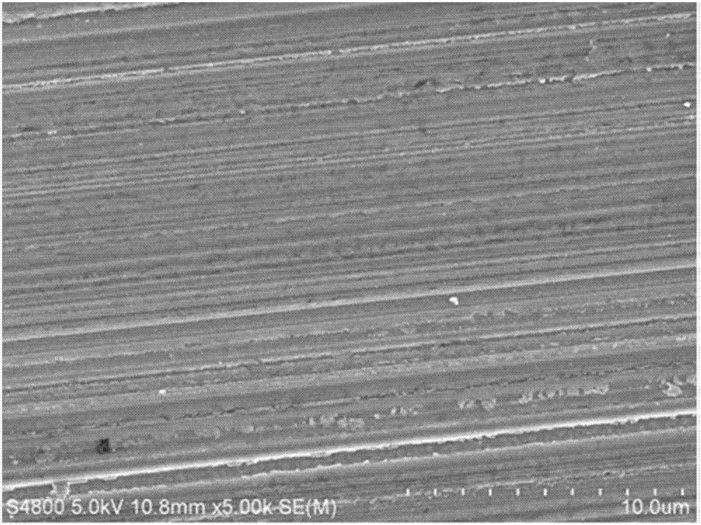
[0032] The first step is to immerse the diamond wire-cut polysilicon wafer in NaOH solution for treatment, remove the mechanical damage layer on the surface of the silicon wafer, take out the silicon wafer and immerse it in an aqueous solution for cleaning, wherein the concentration of NaOH solution is 6%, and the treatment temperature is 55°C , the alkali treatment time is 4min.

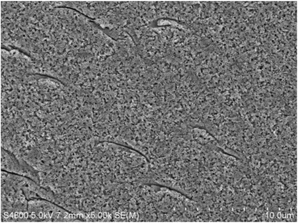
[0033] In the second step, the polysilicon wafer with the mechanically damaged layer removed is placed in a mixed solution of hydrofluoric acid, hydrogen peroxide, metal salts, additives and deionized water for black silicon treatment, that is, metal catalysis, chemical etching, and silver plating are used to dig holes. After integrated processing. The mass fraction of described hydrofluoric acid is 28%, and the mass fraction of hydrogen peroxide is ...

Embodiment 2

[0038] A metal-catalyzed texturing method for reducing the reflectivity of diamond-wire-cut polycrystalline silicon wafers, comprising the steps of:

[0039] The first step is to immerse the diamond wire-cut polysilicon wafer in NaOH solution for treatment, remove the mechanical damage layer on the surface of the silicon wafer, take out the silicon wafer and immerse it in an aqueous solution for cleaning, wherein the concentration of NaOH solution is 8%, and the treatment temperature is 60°C , the alkali treatment time is 3min.

[0040] In the second step, the polysilicon wafer with the mechanically damaged layer removed is placed in a mixed solution of hydrofluoric acid, hydrogen peroxide, metal salt, additives and deionized water for black silicon pretreatment, and metal catalysis and chemical etching are used to dig holes through silver plating After integrated processing. The mass fraction of described hydrofluoric acid is 30%, and the mass fraction of hydrogen peroxide i...

Embodiment 3

[0045] The polysilicon suede sheet of embodiment 1, embodiment 2 and comparative example 1 gained is carried out as follows respectively:

[0046] (1) Put the silicon wafer into the tubular diffusion furnace for diffusion treatment;

[0047] (2) Carry out edge etching and dephosphorous silicon glass treatment to the diffused silicon wafer;

[0048] (3) Deposit silicon nitride anti-reflection film 83nm with the method of tubular PECVD on the front after step (2) treatment;

[0049] (4) Print the back electrode and the aluminum back field on the back, and print the grid line on the front surface of the silicon wafer;

[0050] (5) Sintering to test the electrical properties of the battery sheet.

[0051] The reflectance and electrical properties of the above three different battery sheets were tested, and the obtained results are shown in Table 1 and Table 2.


PUM

PropertyMeasurementUnit
thicknessaaaaaaaaaa
thicknessaaaaaaaaaa
pore sizeaaaaaaaaaa

Abstract

The invention relates to a metal catalytic etching method for decreasing a reflection rate of a polycrystalline silicon wafer cut with a diamond wire. The method comprises the following steps: soaking a polycrystalline silicon wafer cut with a diamond wire in an alkaline solution, and removing a mechanically damaged layer on the surface of the silicon wafer in an etching manner; and integrally treating the treated polycrystalline silicon wafer by virtue of metal catalysis, chemical etching and silver plating and hole digging, and forming a nano porous silicon structure on the surface of the polycrystalline silicon wafer; soaking the polycrystalline silicon wafer treated in the step II in a second mixed solution, performing the etching treatment, so that a honeycomb-shaped suede-like structure is formed on the surface of the silicon wafer; alkaline washing and desilverizing the polycrystalline silicon wafer treated by the last step in an alkaline mixed solution; and cleaning the treated polycrystalline silicon wafer successively with an acid mixed solution and deionized water, and finally drying. By adopting the method, cut marks of the diamond wire can be eliminated, the reflection rate of the polycrystalline silicon etched surface can be effectively decreased to 15 percent, the compatibility with a conventional etching process is good, and the conversion efficiency of a solar cell can be increased.

Description

technical field [0001] The invention belongs to the field of manufacturing polycrystalline silicon solar cells, and in particular relates to a metal-catalyzed texturing method for reducing the reflectivity of polycrystalline silicon slices cut by diamond wires. Background technique [0002] With the rapid development of the industrialized economy and the deterioration of the ecological environment, traditional non-renewable energy sources such as coal, oil, and natural gas are facing a crisis of depletion, and it is imminent to find new renewable energy sources. Among them, solar energy has become a new type of energy to replace traditional petrochemical energy because of its inexhaustibility and inexhaustibility. Solar photovoltaic power generation is the conversion of light energy into electrical energy. Photovoltaic modules have the characteristics of green environmental protection, long service life, low cost, high efficiency and convenience, and have become the focus of...

Claims


Application Information

Patent Timeline
Patent Type & Authority Applications(China)
IPC IPC(8): C30B33/10
CPCC30B33/10
Inventor 管自生侯成成张一源沈志妹刘娟
Owner NANJING NAXIN NEW MATERIAL
Why Eureka
Try Eureka