
Linked furan-based n-type conjugated polymer and its application in organic photoelectric device

A conjugated polymer, polymer technology, applied in the direction of electric solid devices, photovoltaic power generation, electrical components, etc., can solve the problems of low absorption coefficient and insufficient absorption spectrum, and achieve improved absorption coefficient, wide absorption spectrum and absorption. coefficient, effect of high electron mobility

Inactive Publication Date: 2018-03-09
SOUTH CHINA UNIV OF TECH
View PDF1 Cites 3 Cited by
  • Summary
  • Abstract
  • Description
  • Claims
  • Application Information

AI Technical Summary

Problems solved by technology

The main reason is that the absorption coefficient of the existing receptors is not high and the absorption spectrum is not wide enough.

Method used


Image

  • Linked furan-based n-type conjugated polymer and its application in organic photoelectric device
  • Linked furan-based n-type conjugated polymer and its application in organic photoelectric device
  • Linked furan-based n-type conjugated polymer and its application in organic photoelectric device

Examples


Embodiment 1

[0033] A representative synthetic route is as follows:

[0034]

[0035] (1) Monomers M1 and M5 were synthesized according to the method disclosed in the literature [Journal of Materials Chemistry C, 2015, 3(34):8904-8915.].

[0036] (2) Monomers M2, M3, M4, M6, and M7 were synthesized according to the method disclosed in the literature [Journal of the American Chemical Society, 2011, 133(5): 1405-1418.].

[0037] (3) Synthesis of polymers P1, P2, P3:

[0038] Add monomer M1 (0.5mmol) and monomer M2 (0.5mmol) into a 25mL two-necked flask, pass through nitrogen protection, and add 8mL of toluene. Add 5mg Pd(PPh 3 ) 4 , After reacting at 95°C for 12h, the polymer was precipitated with methanol and washed three times. A dark polymer P1 was obtained with a yield of 90.7%.

[0039] Add monomer M1 (0.5 mmol) and monomer M3 (0.5 mmol) into a 25 mL two-necked flask, pass through nitrogen protection, and add 12 mL of toluene. Add 7mg Pd(PPh 3 ) 4 , After reacting at 95°C for...

Embodiment 2

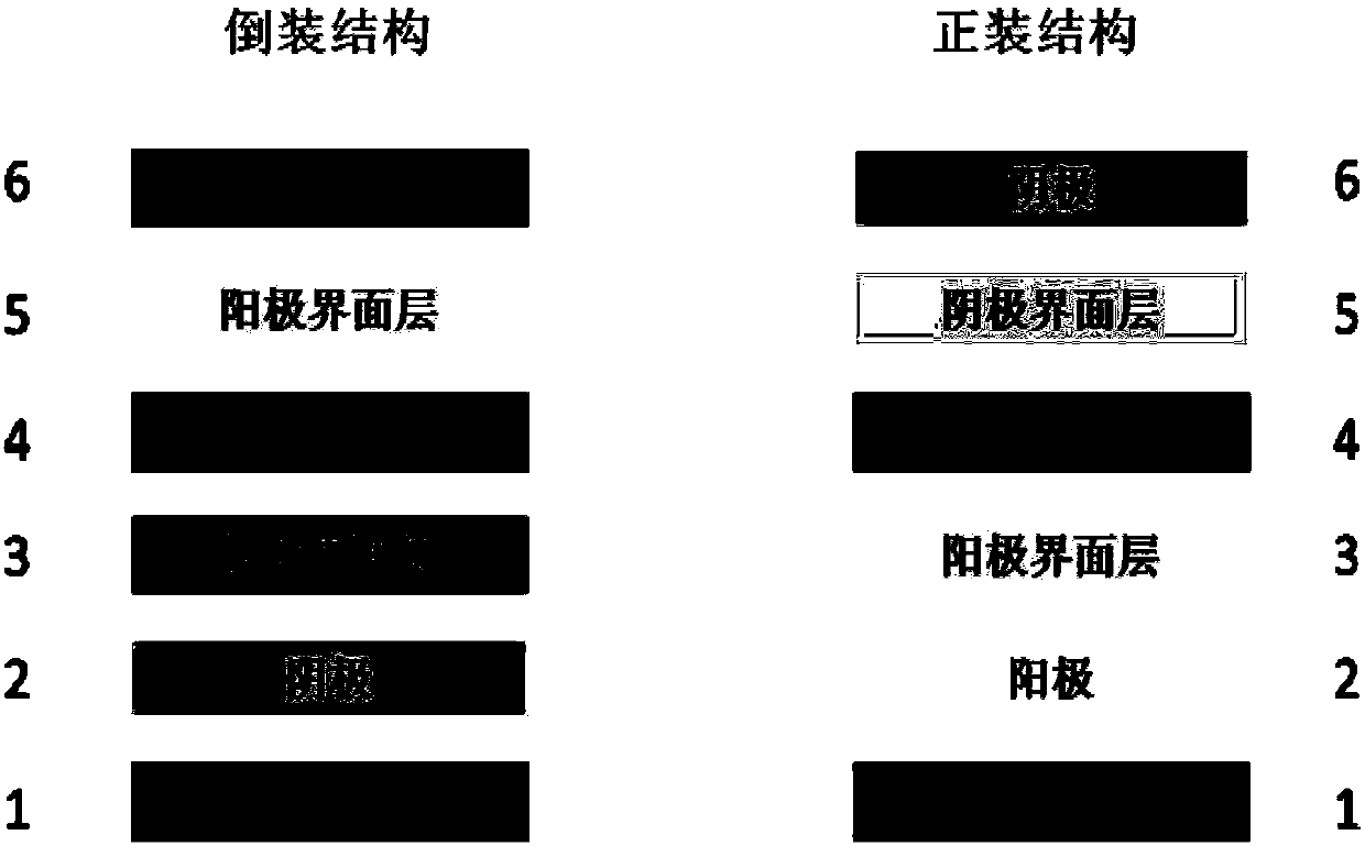
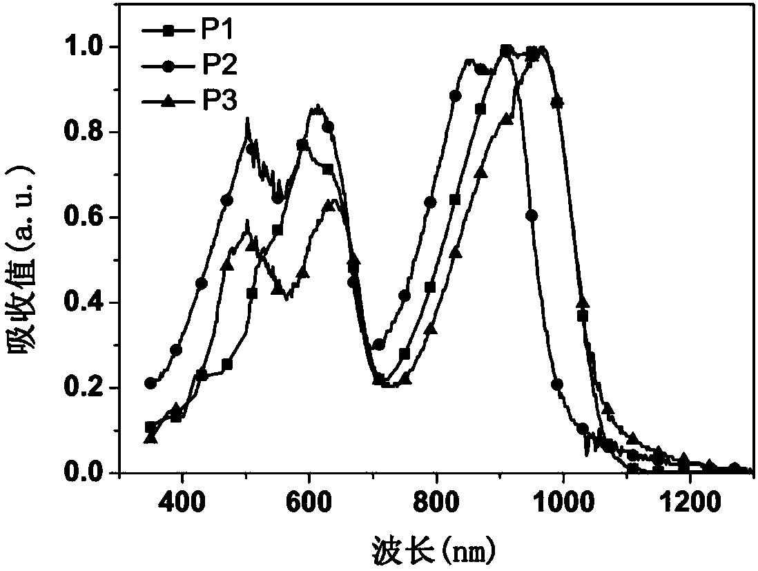
[0046] Using the conjugated polymers P1, P2, and P3 synthesized in Example 1 (the AB components in the structure are the same) as electron acceptors in organic photovoltaic devices (ITO cathode / cathode interface layer / active layer / anode-machine interface layer / anode) middle application

[0047] Pre-cut the ITO conductive glass with a square resistance of 20 ohms / cm2 into 15mm×15mm square pieces. Use acetone, special detergent for micron-sized semiconductors, deionized water, and isopropanol to clean ultrasonically in sequence, blow nitrogen whistle, and place in a constant temperature oven for later use. Spin-coat a layer of 5nm thick PFN-Br on ITO, then spin-coat active layer materials PTB7-Th / P1, PTB7-Th / P2, PTB7-Th / P3 with a thickness of 110nm, and finally evaporate MoO 3 and Al electrodes. All preparations were carried out in a glove box under a nitrogen atmosphere. The current-voltage curves of the fabricated flip-chip devices are as follows: Figure 4 The relevant da...

Embodiment 3

[0049] Using the conjugated polymers P1, P2, and P3 synthesized in Example 1 (with the same AB components in the structure) as electron acceptors in organic photovoltaic devices (ITO anode / anode interface layer / active layer / cathode interface layer / cathode) middle application

[0050] Pre-cut the ITO conductive glass with a square resistance of 20 ohms / cm2 into 15mm×15mm square pieces. Use acetone, special detergent for micron-sized semiconductors, deionized water, and isopropanol to clean ultrasonically in sequence, blow nitrogen whistle, and place in a constant temperature oven for later use. Spin-coat a layer of PEDOT:PSS with a thickness of 20 nm on the ITO, and then spin-coat the active layer materials PTB7-Th / P1, PTB7-Th / P2, and PTB7-Th / P3 with a thickness of 100 nm. Then spin-coat a layer of PFN-Br with a thickness of 5nm, and finally evaporate Al electrodes. All preparations were carried out in a glove box under a nitrogen atmosphere. The current-voltage curves of th...


PUM


Abstract

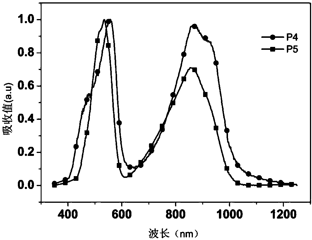
The invention relates to a linked furan-based n-type conjugated polymer and its application in organic photoelectric device. The conjugated polymer is composed of two parts which are naphthalimide andsubstituted linked furan conjugated structure. The conjugated polymer has wide absorption spectrum and absorption coefficient, and high electronic mobility, and can be applied to the high-efficient organic photovoltaic device as the high-efficient electronic acceptor. The invention designs the D-A copolymerized n-type semiconductor conjugated polymer, the conjugated polymer can greatly improve the absorption coefficient of the polymer, widen the absorption spectrum, greatly improve the light current and efficiency of the battery device; the novel n-type conjugated polymer can reach the short-circuited current as the electronic acceptor, and balance an open-circuit voltage and a filling factor; a full polymer photovoltaic device of which energy conversion efficiency is more than 10% is prepared, and is much better than the battery performance of the existed acceptor.

Description

technical field [0001] The invention relates to the field of macromolecular optoelectronic materials, in particular to an n-type conjugated polymer based on the copolymerization of bifuran and naphthalimide based on a main chain structure and its application in organic optoelectronic devices. Background technique [0002] With the increasing global demand for energy, the depletion of traditional energy sources such as oil and coal, and the need to protect the earth's ecological environment, more and more scientists around the world are focusing their research on inexhaustible hydrogen, solar energy, etc. Inexhaustible renewable clean energy. [0003] Mature photovoltaic devices based on inorganic materials such as inorganic silicon, gallium arsenide, and indium phosphide have dominated the market. However, due to their high requirements for material purity, high energy consumption and pollution will occur during processing. And its price is very expensive, so its large-scal...

Claims


Application Information

Patent Timeline
Patent Type & Authority Applications(China)
IPC IPC(8): C08G61/12H01L51/46
CPCC08G61/122C08G61/125C08G2261/91C08G2261/411C08G2261/414C08G2261/3241C08G2261/3222C08G2261/124C08G2261/1424C08G2261/1412C08G2261/18C08G2261/146H10K85/151Y02E10/549
Inventor 黄飞胡志诚应磊曹镛
Owner SOUTH CHINA UNIV OF TECH
Learn More