Method for improving extended wavelength gallium indium arsenide detector etching damage

A technology of indium gallium arsenide and detectors, which is applied in the field of infrared detectors to achieve the effects of reducing density, improving quality and reducing dark current

Inactive Publication Date: 2018-05-04
GUIZHOU ZHENHUA FENGGUANG SEMICON
View PDF2 Cites 7 Cited by
  • Summary
  • Abstract
  • Description
  • Claims
  • Application Information

AI Technical Summary

Problems solved by technology

[0004] The present invention aims to provide a method for improving the etching damage of the extended wavelength InGaAs detector, so as to solve the problem of forming dangling bonds by etching, enhance the passivation effect of the subsequent passivation film, and improve the performance of the device

Method used


Image

  • Method for improving extended wavelength gallium indium arsenide detector etching damage
  • Method for improving extended wavelength gallium indium arsenide detector etching damage

Examples


Embodiment 1

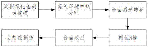
[0030] 1. Deposit silicon nitride etching mask, using plasma enhanced chemical vapor deposition (PECVD) technology to deposit silicon nitride etching mask with a thickness of 600±20nm, the substrate temperature is 330℃±10℃, radio frequency (RF ) power is 40W;

[0031] 2. Heat treatment in a nitrogen environment, put the sample that has deposited silicon nitride etching mask 1 into a rapid thermal annealing furnace, maintain a nitrogen flow rate of 5L / min, fill the annealing furnace with nitrogen for 30s before starting heating, and then The heat treatment is carried out by heating in a nitrogen atmosphere, and the heat treatment conditions are: the temperature is 420°C, and the time is 60s.

[0032] 3. Mesa pattern transfer, the heat-treated sample is subjected to photolithography, the photoresist is AZ1500, and after the photolithography is completed, an ICP etching machine is used to etch the silicon nitride etching mask grown on the epitaxial wafer to complete the patter...

Embodiment 2

[0037] 1. Deposit silicon nitride etching mask, using plasma enhanced chemical vapor deposition (PECVD) technology to deposit silicon nitride etching mask with a thickness of 600±20nm, the substrate temperature is 330±10°C, radio frequency (RF) The power is 40W;

[0038]2. Heat treatment in a nitrogen environment, put the sample that has deposited silicon nitride etching mask 1 into a rapid thermal annealing furnace, maintain a nitrogen flow rate of 5L / min, fill the annealing furnace with nitrogen for 30s before starting heating, and then The heat treatment is carried out by heating in a nitrogen atmosphere, and the heat treatment conditions are: the temperature is 420°C, and the time is 60s.

[0039] 3. Mesa pattern transfer, the heat-treated sample is subjected to photolithography, the photoresist is AZ1500, and after the photolithography is completed, an ICP etching machine is used to etch the silicon nitride etching mask grown on the epitaxial wafer to complete the patt...

Embodiment 3

[0044] 1. Deposit silicon nitride etching mask, using plasma enhanced chemical vapor deposition (PECVD) technology to deposit silicon nitride etching mask with a thickness of 600±20nm, the substrate temperature is 330±10°C, radio frequency (RF) The power is 40W;

[0045] 2. Heat treatment in a nitrogen environment, put the deposited silicon nitride etching mask sample into a rapid thermal annealing furnace, maintain a nitrogen flow rate of 5L / min, fill the annealing furnace with nitrogen for 30s before starting heating, and then Heat treatment under nitrogen atmosphere, heat treatment conditions: temperature 420°C, time 60s.

[0046] 3. Mesa pattern transfer, the heat-treated sample is subjected to photolithography, the photoresist is AZ1500, and after the photolithography is completed, an ICP etching machine is used to etch the silicon nitride etching mask grown on the epitaxial wafer to complete the pattern transfer.

[0047] 4. N-groove etching is performed on the samp...


PUM


Abstract

The invention discloses a method for improving extended wavelength gallium indium arsenide detector etching damage which is provided with a whole set of chip preparation etching processes. The methodincludes the steps: (1) depositing a mask etched by silicon nitride; (2) performing heat treatment in the nitrogen environment; (3) transferring table top images; (4) etching an N groove; (5) forminga table top; (6) removing etching damage. The method has the advantages that the mask etched by the silicon nitride is deposited, the heat treatment is performed in the nitrogen environment, materialdamage can be repaired, complex center density is reduced, material quality is improved, dark current of devices is reduced, hole carrier density can be increased, P-electrode ohmic contact stabilityis facilitated, resistance is reduced, a table top forming process includes gas is etched by the aid of chlorine methane, hydrogen decomposed by the methane in the plasma etching process can passivatedangling bonds formed by etching, and non-radiative recombination center density in materials is reduced. According to an etching damage removing process, damage layers of etching surfaces can be removed, the non-radiative recombination center density is reduced, subsequent passivation effects are enhanced, and the method is applicable to preparation of a high-performance short wave infrared gallium indium arsenide detector.

Description

technical field [0001] The present invention relates to an infrared detector, more particularly to a short-wave infrared InGaAs detector, and in particular to a method for improving etching damage of an extended wavelength InGaAs detector. technical background [0002] It is well known that infrared detectors ( Infrared Detector ) is a device that converts the incident infrared radiation signal into an electrical signal output. Due to the characteristics of low dark current, high detection rate and good radiation resistance of InGaAs at room temperature, InGaAs infrared detectors have shown great application value and are widely used in aerospace and military fields. In the preparation of the extended-wavelength InGaAs short-wave infrared detector chip, the mesa forming process is one of the most critical processes. Because the mesa forming process brings greater lattice damage to the chip material, resulting in deterioration of chip performance. Therefore, for extended-w...

Claims


Application Information

Patent Timeline
Patent Type & Authority Applications(China)
IPC IPC(8): H01L31/09H01L31/18
CPCH01L31/09H01L31/18Y02P70/50
Inventor 李平刘健刘永鹏李政段方高鹏包磊袁兴林夏自金黄丽芳蒋冰桃张小六申林代松井文涛
Owner GUIZHOU ZHENHUA FENGGUANG SEMICON
Why Eureka
Try Eureka