Gallium-nitride-based light emitting diode epitaxial wafer and manufacturing method thereof

A light-emitting diode, gallium nitride-based technology, applied in electrical components, circuits, semiconductor devices, etc., can solve problems such as low luminous efficiency, and achieve the effects of improving luminous efficiency, improving crystal quality, and reducing stress polarization effects.

Active Publication Date: 2018-06-01
HC SEMITEK ZHEJIANG CO LTD
View PDF3 Cites 11 Cited by
  • Summary
  • Abstract
  • Description
  • Claims
  • Application Information

AI Technical Summary

Problems solved by technology

[0006] In order to solve the problem of low luminous efficiency of LEDs under high current density in the prior art, an embodiment of the present invention provides a GaN-based light-emitting diode epitaxial wafer and a manufacturing method thereof

Method used


Image

  • Gallium-nitride-based light emitting diode epitaxial wafer and manufacturing method thereof
  • Gallium-nitride-based light emitting diode epitaxial wafer and manufacturing method thereof

Examples


Embodiment 1

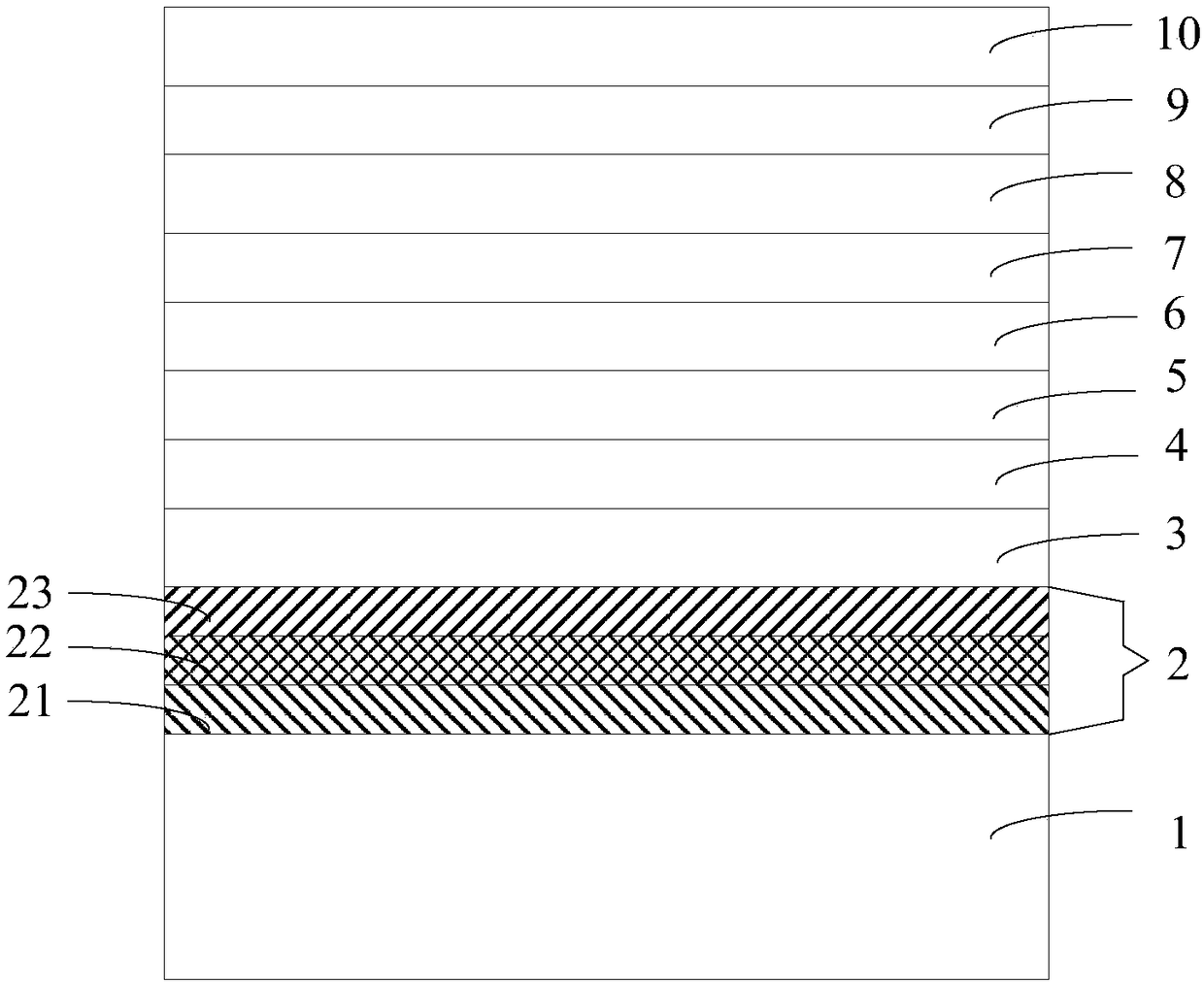
[0028] An embodiment of the present invention provides a GaN-based light-emitting diode epitaxial wafer, figure 1 It is a schematic structural diagram of a gallium nitride-based light-emitting diode epitaxial wafer provided by an embodiment of the present invention, as shown in figure 1 As shown, the gallium nitride-based light-emitting diode includes a substrate 1, and a superlattice buffer layer 2, a high-temperature buffer layer 3, an N-type layer 4, a shallow well layer 5, and a multi-quantum well layer stacked on the substrate 1 in sequence. 6. Low-temperature P-type layer 7 , P-type electron blocking layer 8 , high-temperature P-type layer 9 , and P-type contact layer 10 .

[0029] Wherein, the superlattice buffer layer 2 is a superlattice structure including N periods, and each period of the superlattice structure includes a first sublayer 21, a second sublayer 22, and a third sublayer 22 stacked on the substrate 1. Sublayer 23, N is an integer greater than or equal to...

Embodiment 2

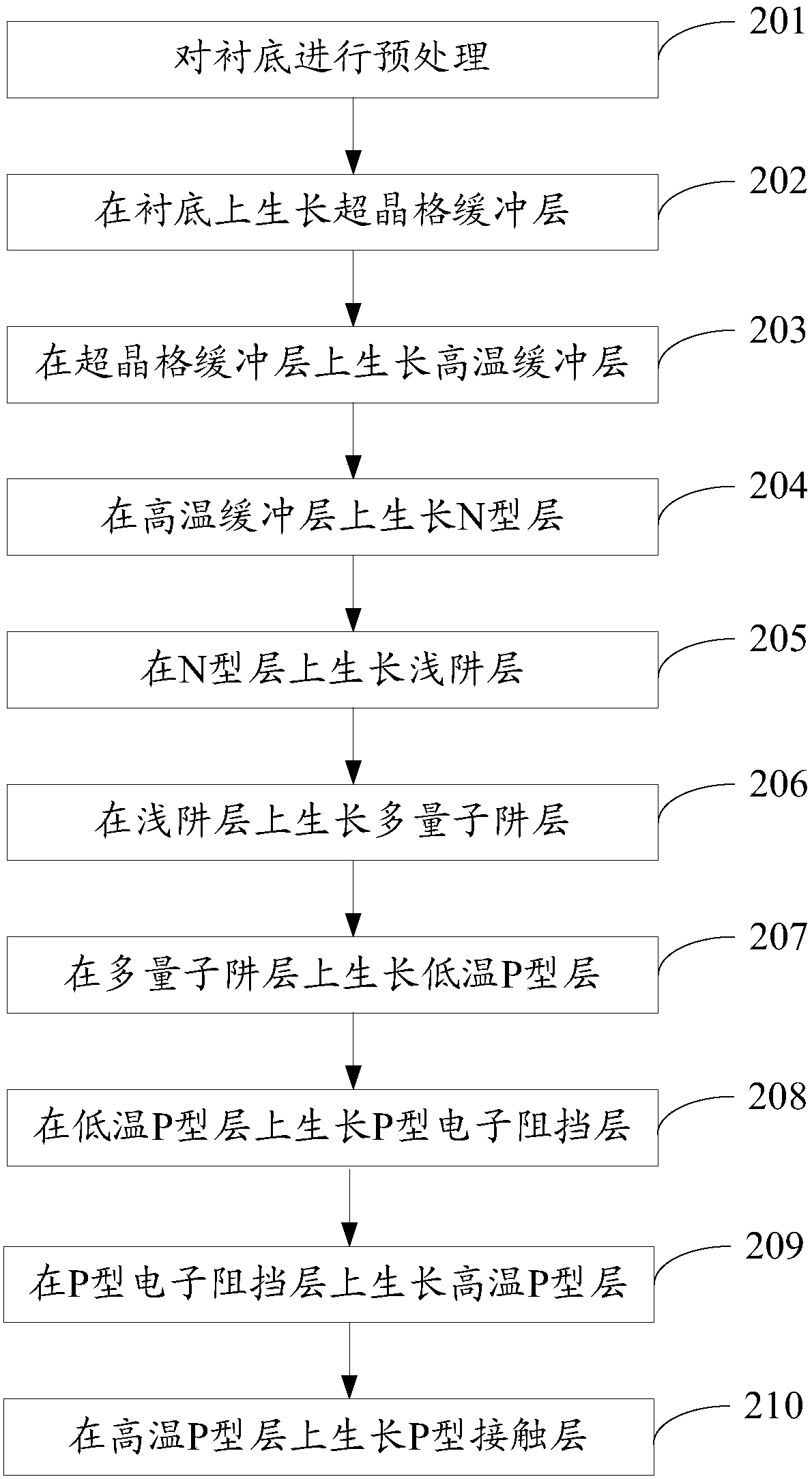
[0042] An embodiment of the present invention provides a method for manufacturing a gallium nitride-based light-emitting diode epitaxial wafer, which is suitable for the gallium nitride-based light-emitting diode epitaxial wafer provided in Embodiment 1. figure 2 It is a flow chart of a method for preparing a gallium nitride-based light-emitting diode epitaxial wafer provided by an embodiment of the present invention, as shown in figure 2 As shown, the manufacturing method includes:

[0043] Step 201, performing pretreatment on the substrate.

[0044] Optionally, the substrate is sapphire with a thickness of 630-650um.

[0045] In this embodiment, Veeco K465i or C4MOCVD (Metal Organic Chemical Vapor Deposition, metal organic compound chemical vapor deposition) equipment is used to realize the LED growth method. Using high-purity H 2 (hydrogen) or high-purity N 2 (nitrogen) or high purity H 2 and high purity N 2 The mixed gas as the carrier gas, high-purity NH 3 As the...

Embodiment 3

[0070] An embodiment of the present invention provides a method for manufacturing a gallium nitride-based light-emitting diode epitaxial wafer. In this embodiment, the superlattice buffer layer is a superlattice structure including N periods, and the superlattice structure of each period It includes the first sublayer, the second sublayer and the third sublayer stacked on the substrate, 1x Ga 1-x N layer, 0.4y Ga 1-y N layer composition, 0.6z Ga 1-z N layer, 0.3

[0071] After finishing the growth of GaN-based light-emitting diode epitaxial wafers, lower the temperature of the reaction chamber to 600-900°C, in PN 2 The atmosphere is annealed for 10-30 minutes, and then gradually lowered to room temperature. Afterwards, a single 9*27mil chip is manufactured through cleaning, deposition, photolithography and etching follow-up processes.

[0072] After XRD (X-ray diffraction, X-ray diffraction) test, it is found that the LED chip provided by the embodiment of the presen...


PUM


Abstract

The invention discloses a gallium-nitride-based light emitting diode epitaxial wafer and a manufacturing method thereof, belonging to the technical field of semiconductors. The gallium-nitride-based light emitting diode epitaxial wafer comprises a superlattice buffer layer, wherein the superlattice buffer layer is of a superlattice structure comprising N periods, and the superlattice structure ofeach period comprises a first sublayer, a second sublayer and a third sublayer which are laminated on a substrate. Through doping Al into the first sub-layer, the lattice mismatch between the substrate and a GaN layer can be alleviated, the defect density can be reduced, and the crystal quality of the entire epitaxial layer can be improved, thereby improving the anti-static capability of an LED. Through doping Mg into the second sublayer, a transition between the first sublayer and the second sublayer can be achieved. Through doping In into the third sublayer, the lattice constant of the thirdsublayer can be increased, thereby accelerating a stress release speed of an N-type layer, reducing the stress polarization effect of a multi-quantum well layer, and increasing the luminous efficiency of the LED.

Description

technical field [0001] The invention relates to the technical field of semiconductors, in particular to a gallium nitride-based light-emitting diode epitaxial wafer and a manufacturing method thereof. Background technique [0002] LED (Light Emitting Diode, Light Emitting Diode) is a semiconductor electronic component that can emit light. As an efficient, environmentally friendly and green new solid-state lighting source, it is being rapidly and widely used, such as traffic lights, car interior and exterior lights, urban landscape lighting, mobile phone backlight, etc. Improving the luminous efficiency of chips is the goal that LEDs are constantly pursuing. [0003] LED epitaxial wafers are an important part of LEDs. Existing gallium nitride-based LEDs include a substrate and an epitaxial layer stacked on the substrate. The epitaxial layer includes a low-temperature buffer layer, a high-temperature buffer layer, and a high-temperature buffer layer stacked on the substrate in...

Claims


Application Information

Patent Timeline
Patent Type & Authority Applications(China)
IPC IPC(8): H01L33/04H01L33/12H01L33/32H01L33/00
CPCH01L33/0075H01L33/04H01L33/12H01L33/32
Inventor 舒辉肖云飞吕蒙普胡加辉李鹏
Owner HC SEMITEK ZHEJIANG CO LTD
Why Eureka
Try Eureka