Infrared detector and preparation method thereof

An infrared detector and superlattice technology, which is applied in the direction of semiconductor devices, final product manufacturing, sustainable manufacturing/processing, etc., can solve the problem of increasing the growth and processing difficulty of barrier type detectors, affecting the stability and reliability of devices, etc. problems, to achieve long-term stability and high reliability, long minority carrier diffusion length, and more processing effects

Active Publication Date: 2018-06-29
苏州晶歌半导体有限公司
View PDF4 Cites 11 Cited by
  • Summary
  • Abstract
  • Description
  • Claims
  • Application Information

AI Technical Summary

Problems solved by technology

Although the device performance of nBn and pMp has a certain improvement compared with traditional devices, because the barrier layer uses aluminum (Al)-containing materials (AlAsSb used in nBn and AlSb used in pMp), and Al is extremely easy to oxidize, Increases the difficulty of growth and processing of barrier detectors, which affects the stability and reliability of the device

Method used


Image

  • Infrared detector and preparation method thereof
  • Infrared detector and preparation method thereof

Examples


preparation example Construction

[0035] The present invention also provides a method for preparing an Al-free pWp barrier type antimonide superlattice infrared detector, which may include the following steps:

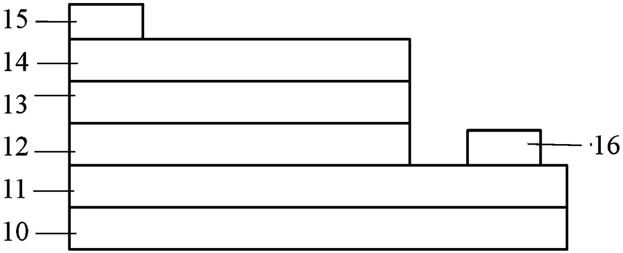
[0036] S1, choose any one of metal-organic chemical vapor deposition and molecular beam epitaxy, and epitaxially grow the p-type InAs / GaSb superlattice lower contact layer 11 and the p-type InAs / GaSb supercrystal on the GaSb or InAs substrate 10 in sequence Lattice absorption layer 12, InGaAs / InAs / InAsSb / InAs / InGaAs superlattice barrier layer 13, and p-type InAs / GaSb superlattice upper contact layer 14.

[0037] S2: Fabricate the mesa on the epitaxial wafer, and deposit a dielectric film to passivate the mesa and sidewall. The mesa is fabricated by any one of wet etching, inductively coupled plasma etching, or reactive ion etching; the dielectric passivation film is formed by plasma enhanced chemical vapor deposition.

[0038] S3: Finally, the electron beam evaporation process is used to deposit the l...

Embodiment 1

[0042] Using Metal Organic Chemical Vapor Deposition (MOCVD) as a growth process, an InAs substrate 10 is provided, and the growth sources are TEGa, TMIn, TMSb and AsH 3 , the p-type dopant source is DEZn. The growth temperature is about 500°C, and the reaction chamber pressure is 100 Torr. After high temperature treatment to remove impurities on the surface of the substrate, according to figure 1 The IR detector structure shown is grown sequentially:

[0043] (1) 100 alternating periods of InAs / GaSb superlattice lower contact layer 11, InAs thickness 4.8nm, GaSb thickness 2.4nm, ie total thickness 0.72μm, Zn doped in InAs and GaSb, the average concentration is 2×10 18 cm -3 ;

[0044] (2) 250 alternating periods of InAs / GaSb superlattice absorption layer 12, the thickness of InAs is 4.8nm, the thickness of GaSb is 2.4nm, that is, the total thickness is 1.8μm, Zn is doped in InAs and GaSb, and the average concentration is 2×10 17 cm -3 ;

[0045] (3) 150 alternating per...

Embodiment 2

[0051] Using molecular beam epitaxy (MBE) as a growth process, a GaSb substrate 10 is provided, the growth source is solid single source Ga, In, As and Sb, and the p-type dopant source is Be. The growth temperature is about 400°C. After the substrate is degassed and impurity removed, according to the following figure 1 The IR detector structure shown is grown sequentially:

[0052] (1) 250 alternating periods of InAs / GaSb superlattice lower contact layer 11, InAs thickness 4.5nm, GaSb thickness 2.1nm, that is, the total thickness 1.65μm, Be doped in InAs and GaSb, the average concentration is 5×10 17 cm -3 ;

[0053] (2) 800 alternating periods of InAs / GaSb superlattice absorption layer 12, InAs thickness 4.5nm, GaSb thickness 2.1nm, that is, the total thickness 5.28μm, Be doped in InAs and GaSb, the average concentration is 5×10 16 cm -3 ;

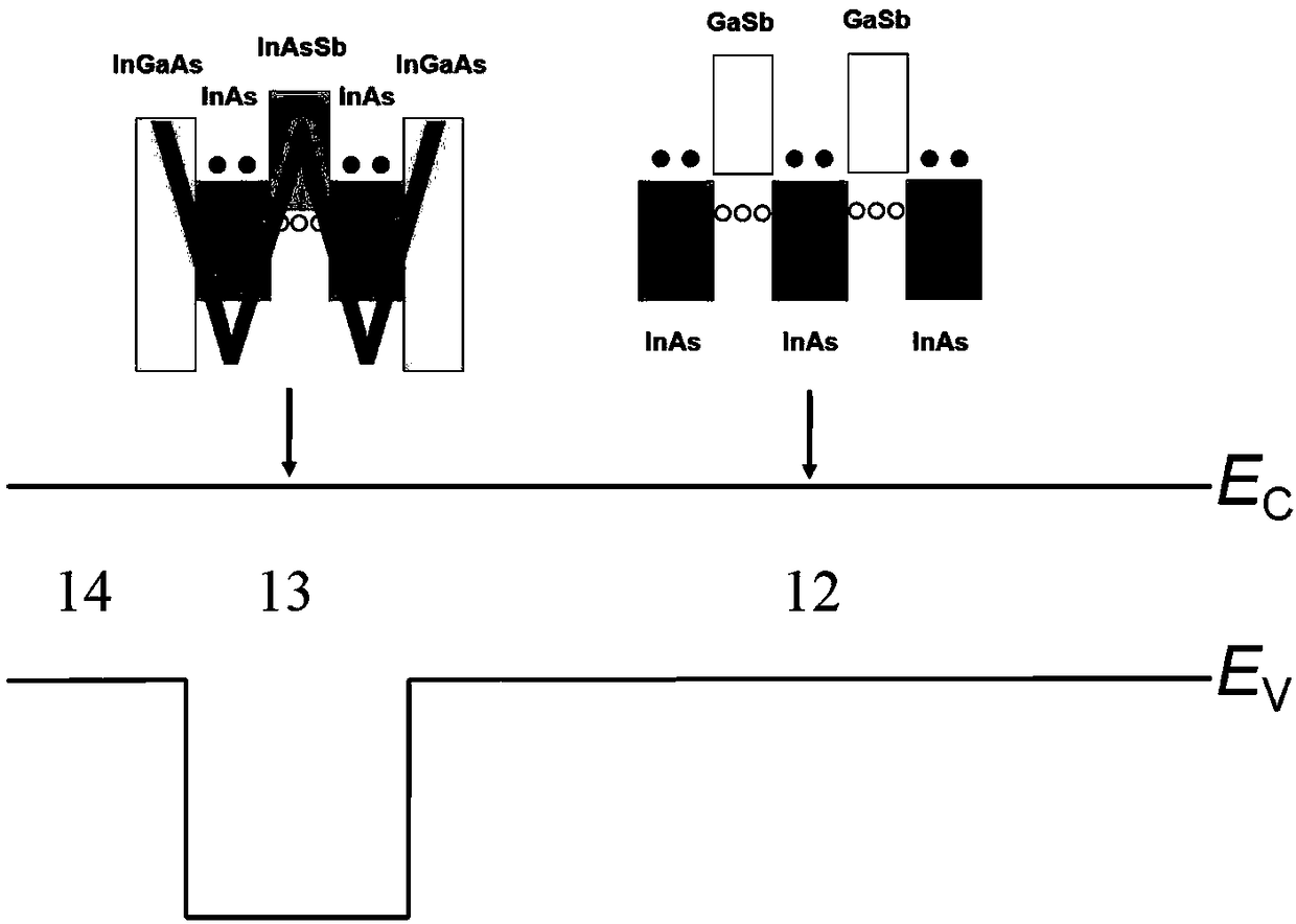
[0054] (3) 250 alternating periods of InGaAs / InAs / InAsSb / InAs / InGaAs superlattice barrier layer 13, wherein the Ga component in In...


PUM


Abstract

The invention relates to the field of semiconductor technologies, and particularly relates to an infrared detector. The infrared detector sequentially comprises a substrate, a p-type InAs / GaSb superlattice lower contact layer, a p-type InAs / GaSb superlattice absorption layer, an InGaAs / InAs / InAsSb / InAs / InGaAs superlattice barrier layer and a p-type InAs / GaSb superlattice upper contact layer from the bottom up, and further comprises a lower electrode arranged at the upper end face of the p-type InAs / GaSb superlattice lower contact layer and an upper electrode arranged at the upper end face of the p-type InAs / GaSb superlattice upper contact layer. The infrared detector adopts Al-free InGaAs / InAs / InAsSb / InAs / InGaAs W-type superlattices to serve as a barrier layer, so that the material is easyto perform epitaxial growth, and the long-term stability and reliability are high.

Description

technical field [0001] The invention relates to the technical field of semiconductors, in particular to a structural improvement of an infrared detector. Background technique [0002] Infrared radiation detection is an important part of infrared technology, widely used in thermal imaging, satellite remote sensing, gas monitoring, optical communication, spectral analysis and other fields. Antimonide InAs / GaSb type II superlattice infrared detectors are considered to be one of the most ideal choices for the preparation of third-generation infrared detectors because of their good uniformity, low Auger recombination rate, and large wavelength adjustment range. Compared with mercury cadmium telluride infrared detector (HgCdTe), it has better uniformity and repeatability, lower cost, and better performance in the very long wavelength band; compared with quantum well infrared detector (QWIP), its quantum efficiency is higher , The dark current is smaller and the process is simpler...

Claims


Application Information

Patent Timeline
Patent Type & Authority Applications(China)
IPC IPC(8): H01L31/0352H01L31/109H01L31/0304H01L31/18
CPCH01L31/0304H01L31/035236H01L31/109H01L31/184Y02P70/50
Inventor 黄勇熊敏杨辉
Owner 苏州晶歌半导体有限公司
Why Eureka
Try Eureka